参数资料
| 型号: | XC4028XL-1BG352I |
| 厂商: | Xilinx Inc |
| 文件页数: | 16/68页 |
| 文件大小: | 0K |
| 描述: | IC FPGA I-TEMP 3.3V 1SPD 352MBGA |
| 产品变化通告: | Product Discontinuation 27/Apr/2010 |
| 标准包装: | 1 |
| 系列: | XC4000E/X |
| LAB/CLB数: | 1024 |
| 逻辑元件/单元数: | 2432 |
| RAM 位总计: | 32768 |
| 输入/输出数: | 256 |
| 门数: | 28000 |
| 电源电压: | 3 V ~ 3.6 V |
| 安装类型: | 表面贴装 |
| 工作温度: | -40°C ~ 100°C |
| 封装/外壳: | 352-LBGA,金属 |
| 供应商设备封装: | 352-MBGA(35x35) |
第1页第2页第3页第4页第5页第6页第7页第8页第9页第10页第11页第12页第13页第14页第15页当前第16页第17页第18页第19页第20页第21页第22页第23页第24页第25页第26页第27页第28页第29页第30页第31页第32页第33页第34页第35页第36页第37页第38页第39页第40页第41页第42页第43页第44页第45页第46页第47页第48页第49页第50页第51页第52页第53页第54页第55页第56页第57页第58页第59页第60页第61页第62页第63页第64页第65页第66页第67页第68页
R
May 14, 1999 (Version 1.6)
6-27
XC4000E and XC4000X Series Field Programmable Gate Arrays
6
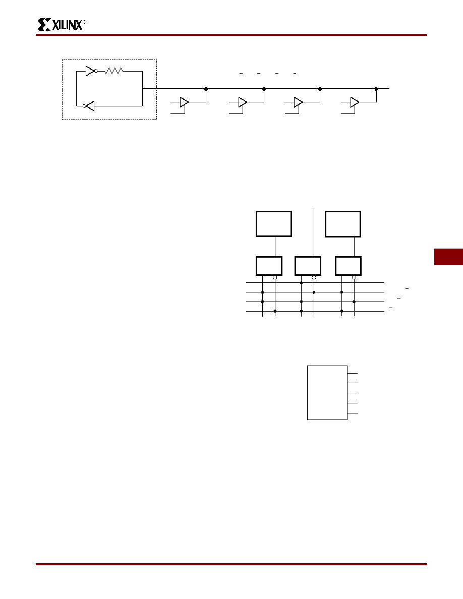
Wide Edge Decoders
Dedicated decoder circuitry boosts the performance of
wide decoding functions. When the address or data eld is
wider than the function generator inputs, FPGAs need
multi-level decoding and are thus slower than PALs.
XC4000 Series CLBs have nine inputs. Any decoder of up
to nine inputs is, therefore, compact and fast. However,
there is also a need for much wider decoders, especially for
address decoding in large microprocessor systems.
An XC4000 Series FPGA has four programmable decoders
located on each edge of the device. The inputs to each
decoder are any of the IOB I1 signals on that edge plus one
local interconnect per CLB row or column. Each row or col-
umn of CLBs provides up to three variables or their compli-
ments., as shown in Figure 23. Each decoder generates a
High output (resistor pull-up) when the AND condition of
the selected inputs, or their complements, is true. This is
analogous to a product term in typical PAL devices.
Each of these wired-AND gates is capable of accepting up
to 42 inputs on the XC4005E and 72 on the XC4013E.
There are up to 96 inputs for each decoder on the
XC4028X and 132 on the XC4052X.
The decoders may
also be split in two when a larger number of narrower
decoders are required, for a maximum of 32 decoders per
device.
The decoder outputs can drive CLB inputs, so they can be
combined with other logic to form a PAL-like AND/OR struc-
ture. The decoder outputs can also be routed directly to the
chip outputs. For fastest speed, the output should be on the
same chip edge as the decoder. Very large PALs can be
emulated by ORing the decoder outputs in a CLB. This
decoding feature covers what has long been considered a
weakness of older FPGAs. Users often resorted to external
PALs for simple but fast decoding functions. Now, the dedi-
cated decoders in the XC4000 Series device can imple-
ment these functions fast and efciently.
To use the wide edge decoders, place one or more of the
WAND library symbols (WAND1, WAND4, WAND8,
WAND16). Attach a DECODE attribute or property to each
WAND symbol. Tie the outputs together and attach a PUL-
LUP symbol. Location attributes or properties such as L
(left edge) or TR (right half of top edge) should also be used
to ensure the correct placement of the decoder inputs.
On-Chip Oscillator
XC4000 Series devices include an internal oscillator. This
oscillator is used to clock the power-on time-out, for cong-
uration memory clearing, and as the source of CCLK in
Master conguration modes. The oscillator runs at a nomi-
nal 8 MHz frequency that varies with process, Vcc, and
temperature. The output frequency falls between 4 and 10
MHz.
D
N
D
C
D
B
D
A
AB
C
N
Z = D
A
A + D
B
B + D
C
C + D
N
N
~100 k
"Weak Keeper"
X6466
BUFT
Figure 22: 3-State Buffers Implement a Multiplexer
IOB
B
A
INTERCONNECT
(
C) .....
(A B C) .....
.I1
X2627
C
Figure 23: XC4000 Series Edge Decoding Example
F16K
F500K
F8M
F490
F15
X6703
OSC4
Figure 24: XC4000 Series Oscillator Symbol
Product Obsolete or Under Obsolescence
相关PDF资料 |
PDF描述 |
|---|---|
| IDT709359L7PF | IC SRAM 144KBIT 7NS 100TQFP |
| KMC7448HX1400ND | IC MPU 128BIT 1400MHZ 360-FCCBGA |
| MC7447ATHX1167NB | IC MPU RISC 1167MHZ 360-FCCBGA |
| IDT709169L7PF | IC SRAM 144KBIT 7NS 100TQFP |
| MC68040RC40A | IC MICROPROCESSOR 32BIT 179-PGA |
相关代理商/技术参数 |
参数描述 |
|---|---|
| XC4028XL-1HQ160C | 功能描述:IC FPGA C-TEMP 3.3V 1SPD 160HQFP RoHS:否 类别:集成电路 (IC) >> 嵌入式 - FPGA(现场可编程门阵列) 系列:XC4000E/X 标准包装:1 系列:Kintex-7 LAB/CLB数:25475 逻辑元件/单元数:326080 RAM 位总计:16404480 输入/输出数:350 门数:- 电源电压:0.97 V ~ 1.03 V 安装类型:表面贴装 工作温度:0°C ~ 85°C 封装/外壳:900-BBGA,FCBGA 供应商设备封装:900-FCBGA(31x31) 其它名称:122-1789 |
| XC4028XL-1HQ160I | 功能描述:IC FPGA I-TEMP 3.3V 1SPD 160HQFP RoHS:否 类别:集成电路 (IC) >> 嵌入式 - FPGA(现场可编程门阵列) 系列:XC4000E/X 标准包装:1 系列:Kintex-7 LAB/CLB数:25475 逻辑元件/单元数:326080 RAM 位总计:16404480 输入/输出数:350 门数:- 电源电压:0.97 V ~ 1.03 V 安装类型:表面贴装 工作温度:0°C ~ 85°C 封装/外壳:900-BBGA,FCBGA 供应商设备封装:900-FCBGA(31x31) 其它名称:122-1789 |
| XC4028XL-1HQ208C | 功能描述:IC FPGA C-TEMP 3.3V 1SPD 208HQFP RoHS:否 类别:集成电路 (IC) >> 嵌入式 - FPGA(现场可编程门阵列) 系列:XC4000E/X 标准包装:1 系列:Kintex-7 LAB/CLB数:25475 逻辑元件/单元数:326080 RAM 位总计:16404480 输入/输出数:350 门数:- 电源电压:0.97 V ~ 1.03 V 安装类型:表面贴装 工作温度:0°C ~ 85°C 封装/外壳:900-BBGA,FCBGA 供应商设备封装:900-FCBGA(31x31) 其它名称:122-1789 |
| XC4028XL-1HQ208C0907 | 制造商:Xilinx 功能描述: |
| XC4028XL-1HQ208I | 功能描述:IC FPGA I-TEMP 3.3V 1SPD 208HQFP RoHS:否 类别:集成电路 (IC) >> 嵌入式 - FPGA(现场可编程门阵列) 系列:XC4000E/X 标准包装:1 系列:Kintex-7 LAB/CLB数:25475 逻辑元件/单元数:326080 RAM 位总计:16404480 输入/输出数:350 门数:- 电源电压:0.97 V ~ 1.03 V 安装类型:表面贴装 工作温度:0°C ~ 85°C 封装/外壳:900-BBGA,FCBGA 供应商设备封装:900-FCBGA(31x31) 其它名称:122-1789 |
发布紧急采购,3分钟左右您将得到回复。