参数资料
| 型号: | XC4028XL-1HQ160I |
| 厂商: | Xilinx Inc |
| 文件页数: | 14/68页 |
| 文件大小: | 0K |
| 描述: | IC FPGA I-TEMP 3.3V 1SPD 160HQFP |
| 产品变化通告: | XC4000(XL,XLA,E) Discontinuation 15/Nov/2004 |
| 标准包装: | 24 |
| 系列: | XC4000E/X |
| LAB/CLB数: | 1024 |
| 逻辑元件/单元数: | 2432 |
| RAM 位总计: | 32768 |
| 输入/输出数: | 129 |
| 门数: | 28000 |
| 电源电压: | 3 V ~ 3.6 V |
| 安装类型: | 表面贴装 |
| 工作温度: | -40°C ~ 100°C |
| 封装/外壳: | 160-BQFP 裸露焊盘 |
| 供应商设备封装: | 160-PQFP(28x28) |
第1页第2页第3页第4页第5页第6页第7页第8页第9页第10页第11页第12页第13页当前第14页第15页第16页第17页第18页第19页第20页第21页第22页第23页第24页第25页第26页第27页第28页第29页第30页第31页第32页第33页第34页第35页第36页第37页第38页第39页第40页第41页第42页第43页第44页第45页第46页第47页第48页第49页第50页第51页第52页第53页第54页第55页第56页第57页第58页第59页第60页第61页第62页第63页第64页第65页第66页第67页第68页
R
May 14, 1999 (Version 1.6)
6-25
XC4000E and XC4000X Series Field Programmable Gate Arrays
6
Output Multiplexer/2-Input Function Generator
(XC4000X only)
As shown in Figure 16 on page 21, the output path in the
XC4000X IOB contains an additional multiplexer not avail-
able in the XC4000E IOB. The multiplexer can also be con-
gured as a 2-input function generator, implementing a
pass-gate, AND-gate, OR-gate, or XOR-gate, with 0, 1, or 2
inverted inputs. The logic used to implement these func-
tions is shown in the upper gray area of Figure 16.
When congured as a multiplexer, this feature allows two
output signals to time-share the same output pad; effec-
tively doubling the number of device outputs without requir-
ing a larger, more expensive package.
When the MUX is congured as a 2-input function genera-
tor, logic can be implemented within the IOB itself. Com-
bined with a Global Early buffer, this arrangement allows
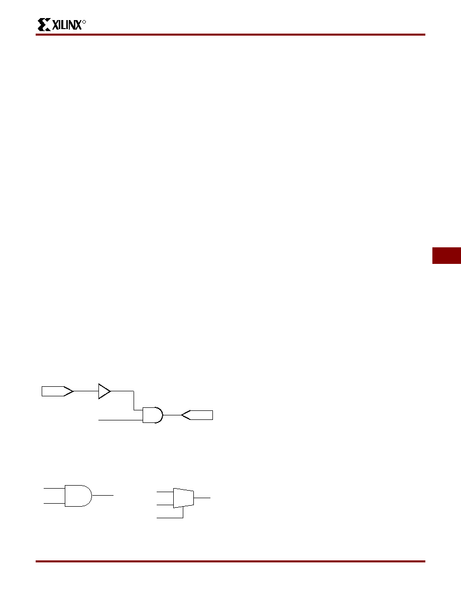
very high-speed gating of a single signal. For example, a
wide decoder can be implemented in CLBs, and its output
gated with a Read or Write Strobe Driven by a BUFGE
buffer, as shown in Figure 19. The critical-path pin-to-pin
delay of this circuit is less than 6 nanoseconds.
As shown in Figure 16, the IOB input pins Out, Output
Clock, and Clock Enable have different delays and different
exibilities regarding polarity. Additionally, Output Clock
sources are more limited than the other inputs. Therefore,
the Xilinx software does not move logic into the IOB func-
tion generators unless explicitly directed to do so.
The user can specify that the IOB function generator be
used, by placing special library symbols beginning with the
letter “O.” For example, a 2-input AND-gate in the IOB func-
tion generator is called OAND2. Use the symbol input pin
labelled “F” for the signal on the critical path. This signal is
placed on the OK pin — the IOB input with the shortest
delay to the function generator. Two examples are shown in
Other IOB Options
There are a number of other programmable options in the
XC4000 Series IOB.
Pull-up and Pull-down Resistors
Programmable pull-up and pull-down resistors are useful
for tying unused pins to Vcc or Ground to minimize power
consumption and reduce noise sensitivity. The congurable
pull-up resistor is a p-channel transistor that pulls to Vcc.
The congurable pull-down resistor is an n-channel transis-
tor that pulls to Ground.
The value of these resistors is 50 k
100 k. This high
value makes them unsuitable as wired-AND pull-up resis-
tors.
The pull-up resistors for most user-programmable IOBs are
active during the conguration process. See Table 22 on
page 58 for a list of pins with pull-ups active before and dur-
ing conguration.
After conguration, voltage levels of unused pads, bonded
or un-bonded, must be valid logic levels, to reduce noise
sensitivity and avoid excess current. Therefore, by default,
unused pads are congured with the internal pull-up resis-
tor active. Alternatively, they can be individually congured
with the pull-down resistor, or as a driven output, or to be
driven by an external source. To activate the internal
pull-up, attach the PULLUP library component to the net
attached to the pad. To activate the internal pull-down,
attach the PULLDOWN library component to the net
attached to the pad.
Independent Clocks
Separate clock signals are provided for the input and output
ip-ops. The clock can be independently inverted for each
ip-op within the IOB, generating either falling-edge or ris-
ing-edge triggered ip-ops. The clock inputs for each IOB
are independent, except that in the XC4000X, the Fast
Capture latch shares an IOB input with the output clock pin.
Early Clock for IOBs (XC4000X only)
Special early clocks are available for IOBs. These clocks
are sourced by the same sources as the Global Low-Skew
buffers, but are separately buffered. They have fewer loads
and therefore less delay. The early clock can drive either
the IOB output clock or the IOB input clock, or both. The
early clock allows fast capture of input data, and fast
clock-to-output on output data. The Global Early buffers
that drive these clocks are described in “Global Nets and
Global Set/Reset
As with the CLB registers, the Global Set/Reset signal
(GSR) can be used to set or clear the input and output reg-
isters, depending on the value of the INIT attribute or prop-
erty. The two ip-ops can be individually congured to set
IPAD
F
OPAD
FAST
BUFGE
OAND2
from
internal
logic
X9019
Figure 19: Fast Pin-to-Pin Path in XC4000X
OAND2
F
X6598
D0
S0
D1
O
OMUX2
X6599
Figure 20: AND & MUX Symbols in XC4000X IOB
Product Obsolete or Under Obsolescence
相关PDF资料 |
PDF描述 |
|---|---|
| EEC60DTEI | CONN EDGECARD 120POS .100 EYELET |
| IDT71V3556SA150BGG8 | IC SRAM 4MBIT 150MHZ 119BGA |
| IDT71V3556SA133BGG8 | IC SRAM 4MBIT 133MHZ 119BGA |
| IDT71V3556SA100BGG8 | IC SRAM 4MBIT 100MHZ 119BGA |
| IDT71V416L15BEGI | IC SRAM 4MBIT 15NS 48FBGA |
相关代理商/技术参数 |
参数描述 |
|---|---|
| XC4028XL-1HQ208C | 功能描述:IC FPGA C-TEMP 3.3V 1SPD 208HQFP RoHS:否 类别:集成电路 (IC) >> 嵌入式 - FPGA(现场可编程门阵列) 系列:XC4000E/X 标准包装:1 系列:Kintex-7 LAB/CLB数:25475 逻辑元件/单元数:326080 RAM 位总计:16404480 输入/输出数:350 门数:- 电源电压:0.97 V ~ 1.03 V 安装类型:表面贴装 工作温度:0°C ~ 85°C 封装/外壳:900-BBGA,FCBGA 供应商设备封装:900-FCBGA(31x31) 其它名称:122-1789 |
| XC4028XL-1HQ208C0907 | 制造商:Xilinx 功能描述: |
| XC4028XL-1HQ208I | 功能描述:IC FPGA I-TEMP 3.3V 1SPD 208HQFP RoHS:否 类别:集成电路 (IC) >> 嵌入式 - FPGA(现场可编程门阵列) 系列:XC4000E/X 标准包装:1 系列:Kintex-7 LAB/CLB数:25475 逻辑元件/单元数:326080 RAM 位总计:16404480 输入/输出数:350 门数:- 电源电压:0.97 V ~ 1.03 V 安装类型:表面贴装 工作温度:0°C ~ 85°C 封装/外壳:900-BBGA,FCBGA 供应商设备封装:900-FCBGA(31x31) 其它名称:122-1789 |
| XC4028XL-1HQ240C | 功能描述:IC FPGA C-TEMP 3.3V 1SPD 240HQFP RoHS:否 类别:集成电路 (IC) >> 嵌入式 - FPGA(现场可编程门阵列) 系列:XC4000E/X 标准包装:1 系列:Kintex-7 LAB/CLB数:25475 逻辑元件/单元数:326080 RAM 位总计:16404480 输入/输出数:350 门数:- 电源电压:0.97 V ~ 1.03 V 安装类型:表面贴装 工作温度:0°C ~ 85°C 封装/外壳:900-BBGA,FCBGA 供应商设备封装:900-FCBGA(31x31) 其它名称:122-1789 |
| XC4028XL-1HQ240I | 功能描述:IC FPGA I-TEMP 3.3V 1SPD 240HQFP RoHS:否 类别:集成电路 (IC) >> 嵌入式 - FPGA(现场可编程门阵列) 系列:XC4000E/X 标准包装:1 系列:Kintex-7 LAB/CLB数:25475 逻辑元件/单元数:326080 RAM 位总计:16404480 输入/输出数:350 门数:- 电源电压:0.97 V ~ 1.03 V 安装类型:表面贴装 工作温度:0°C ~ 85°C 封装/外壳:900-BBGA,FCBGA 供应商设备封装:900-FCBGA(31x31) 其它名称:122-1789 |
发布紧急采购,3分钟左右您将得到回复。