参数资料
| 型号: | XC4028XL-1HQ208C |
| 厂商: | Xilinx Inc |
| 文件页数: | 18/68页 |
| 文件大小: | 0K |
| 描述: | IC FPGA C-TEMP 3.3V 1SPD 208HQFP |
| 产品变化通告: | Product Discontinuation 19/Feb/2007 |
| 标准包装: | 1 |
| 系列: | XC4000E/X |
| LAB/CLB数: | 1024 |
| 逻辑元件/单元数: | 2432 |
| RAM 位总计: | 32768 |
| 输入/输出数: | 160 |
| 门数: | 28000 |
| 电源电压: | 3 V ~ 3.6 V |
| 安装类型: | 表面贴装 |
| 工作温度: | 0°C ~ 85°C |
| 封装/外壳: | 208-BFQFP 裸露焊盘 |
| 供应商设备封装: | 208-PQFP(28x28) |
第1页第2页第3页第4页第5页第6页第7页第8页第9页第10页第11页第12页第13页第14页第15页第16页第17页当前第18页第19页第20页第21页第22页第23页第24页第25页第26页第27页第28页第29页第30页第31页第32页第33页第34页第35页第36页第37页第38页第39页第40页第41页第42页第43页第44页第45页第46页第47页第48页第49页第50页第51页第52页第53页第54页第55页第56页第57页第58页第59页第60页第61页第62页第63页第64页第65页第66页第67页第68页
R
May 14, 1999 (Version 1.6)
6-29
XC4000E and XC4000X Series Field Programmable Gate Arrays
6
Table 14: Routing per CLB in XC4000 Series Devices
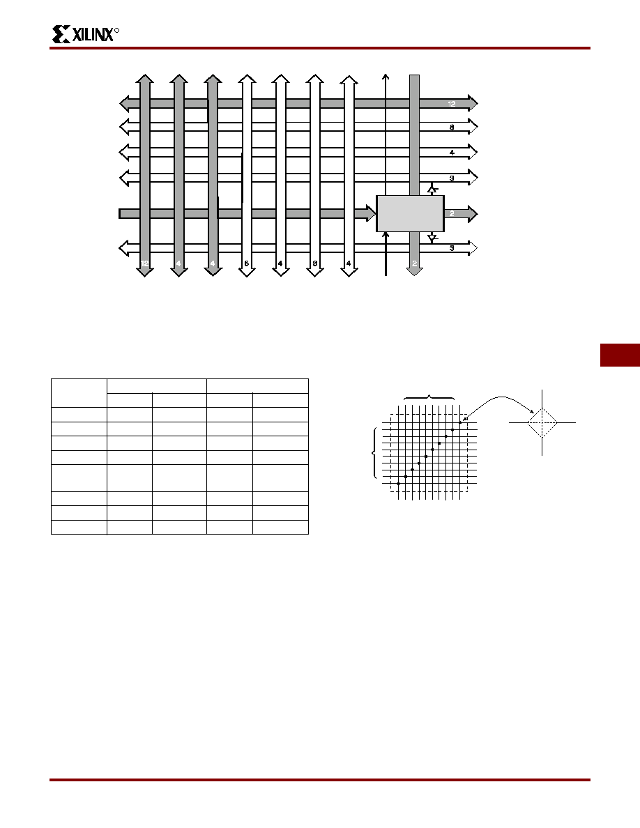
Programmable Switch Matrices
The horizontal and vertical single- and double-length lines
intersect at a box called a programmable switch matrix
(PSM). Each switch matrix consists of programmable pass
transistors used to establish connections between the lines
(see Figure 26).
For example, a single-length signal entering on the right
side of the switch matrix can be routed to a single-length
line on the top, left, or bottom sides, or any combination
thereof, if multiple branches are required. Similarly, a dou-
ble-length signal can be routed to a double-length line on
any or all of the other three edges of the programmable
switch matrix.
Single-Length Lines
Single-length lines provide the greatest interconnect exi-
bility and offer fast routing between adjacent blocks. There
are eight vertical and eight horizontal single-length lines
associated with each CLB. These lines connect the switch-
ing matrices that are located in every row and a column of
CLBs.
Single-length lines are connected by way of the program-
mable switch matrices, as shown in Figure 28. Routing
connectivity is shown in Figure 27.
Single-length lines incur a delay whenever they go through
a switching matrix. Therefore, they are not suitable for rout-
ing signals for long distances. They are normally used to
conduct signals within a localized area and to provide the
branching for nets with fanout greater than one.
x5994
Quad
Single
Double
Long
Direct
Connect
Long
CLB
Long
Global
Clock
Long
Double Single
Global
Clock
Carry
Chain
Direct
Connect
Figure 25: High-Level Routing Diagram of XC4000 Series CLB (shaded arrows indicate XC4000X only)
XC4000E
XC4000X
Vertical Horizontal Vertical Horizontal
Singles
8
Doubles
4
Quads
0
12
Longlines
6
10
6
Direct
Connects
00
2
Globals
4
0
8
0
Carry Logic
2
0
1
0
Total
24
18
45
32
Six Pass Transistors
Per Switch Matrix
Interconnect Point
Singles
Double
Singles
Double
X6600
Figure 26: Programmable Switch Matrix (PSM)
Product Obsolete or Under Obsolescence
相关PDF资料 |
PDF描述 |
|---|---|
| RSC65DRAH-S734 | CONN EDGECARD 130PS .100 R/A PCB |
| RMC65DRAH-S734 | CONN EDGECARD 130PS .100 R/A PCB |
| ACB64DHBS | CONN EDGECARD 128PS R/A .050 DIP |
| ASC49DRAS | CONN EDGECARD 98POS .100 R/A DIP |
| ACB110DHRR | CONN CARD EXTEND 220POS .050" |
相关代理商/技术参数 |
参数描述 |
|---|---|
| XC4028XL-1HQ208C0907 | 制造商:Xilinx 功能描述: |
| XC4028XL-1HQ208I | 功能描述:IC FPGA I-TEMP 3.3V 1SPD 208HQFP RoHS:否 类别:集成电路 (IC) >> 嵌入式 - FPGA(现场可编程门阵列) 系列:XC4000E/X 标准包装:1 系列:Kintex-7 LAB/CLB数:25475 逻辑元件/单元数:326080 RAM 位总计:16404480 输入/输出数:350 门数:- 电源电压:0.97 V ~ 1.03 V 安装类型:表面贴装 工作温度:0°C ~ 85°C 封装/外壳:900-BBGA,FCBGA 供应商设备封装:900-FCBGA(31x31) 其它名称:122-1789 |
| XC4028XL-1HQ240C | 功能描述:IC FPGA C-TEMP 3.3V 1SPD 240HQFP RoHS:否 类别:集成电路 (IC) >> 嵌入式 - FPGA(现场可编程门阵列) 系列:XC4000E/X 标准包装:1 系列:Kintex-7 LAB/CLB数:25475 逻辑元件/单元数:326080 RAM 位总计:16404480 输入/输出数:350 门数:- 电源电压:0.97 V ~ 1.03 V 安装类型:表面贴装 工作温度:0°C ~ 85°C 封装/外壳:900-BBGA,FCBGA 供应商设备封装:900-FCBGA(31x31) 其它名称:122-1789 |
| XC4028XL-1HQ240I | 功能描述:IC FPGA I-TEMP 3.3V 1SPD 240HQFP RoHS:否 类别:集成电路 (IC) >> 嵌入式 - FPGA(现场可编程门阵列) 系列:XC4000E/X 标准包装:1 系列:Kintex-7 LAB/CLB数:25475 逻辑元件/单元数:326080 RAM 位总计:16404480 输入/输出数:350 门数:- 电源电压:0.97 V ~ 1.03 V 安装类型:表面贴装 工作温度:0°C ~ 85°C 封装/外壳:900-BBGA,FCBGA 供应商设备封装:900-FCBGA(31x31) 其它名称:122-1789 |
| XC4028XL-1HQ304C | 功能描述:IC FPGA C-TEMP 3.3V 1SPD 304HQFP RoHS:否 类别:集成电路 (IC) >> 嵌入式 - FPGA(现场可编程门阵列) 系列:XC4000E/X 标准包装:1 系列:Kintex-7 LAB/CLB数:25475 逻辑元件/单元数:326080 RAM 位总计:16404480 输入/输出数:350 门数:- 电源电压:0.97 V ~ 1.03 V 安装类型:表面贴装 工作温度:0°C ~ 85°C 封装/外壳:900-BBGA,FCBGA 供应商设备封装:900-FCBGA(31x31) 其它名称:122-1789 |
发布紧急采购,3分钟左右您将得到回复。