参数资料
| 型号: | XC4036XL-2HQ240I |
| 厂商: | Xilinx Inc |
| 文件页数: | 28/68页 |
| 文件大小: | 0K |
| 描述: | IC FPGA I-TEMP 3.3V 2SPD 240HQFP |
| 产品变化通告: | XC4000(XL,XLA,E) Discontinuation 15/Nov/2004 |
| 标准包装: | 24 |
| 系列: | XC4000E/X |
| LAB/CLB数: | 1296 |
| 逻辑元件/单元数: | 3078 |
| RAM 位总计: | 41472 |
| 输入/输出数: | 193 |
| 门数: | 36000 |
| 电源电压: | 3 V ~ 3.6 V |
| 安装类型: | 表面贴装 |
| 工作温度: | -40°C ~ 100°C |
| 封装/外壳: | 240-BFQFP 裸露焊盘 |
| 供应商设备封装: | 240-PQFP(32x32) |
第1页第2页第3页第4页第5页第6页第7页第8页第9页第10页第11页第12页第13页第14页第15页第16页第17页第18页第19页第20页第21页第22页第23页第24页第25页第26页第27页当前第28页第29页第30页第31页第32页第33页第34页第35页第36页第37页第38页第39页第40页第41页第42页第43页第44页第45页第46页第47页第48页第49页第50页第51页第52页第53页第54页第55页第56页第57页第58页第59页第60页第61页第62页第63页第64页第65页第66页第67页第68页
R
XC4000E and XC4000X Series Field Programmable Gate Arrays
6-38
May 14, 1999 (Version 1.6)
Global Early Buffers
Each corner of the XC4000X device has two Global Early
buffers. The primary purpose of the Global Early buffers is
to provide an earlier clock access than the potentially
heavily-loaded Global Low-Skew buffers. A clock source
applied to both buffers will result in the Global Early clock
edge occurring several nanoseconds earlier than the Glo-
bal Low-Skew buffer clock edge, due to the lighter loading.
Global Early buffers also facilitate the fast capture of device
inputs, using the Fast Capture latches described in “IOB
Input Signals” on page 20. For Fast Capture, take a single
clock signal, and route it through both a Global Early buffer
and a Global Low-Skew buffer. (The two buffers share an
input pad.) Use the Global Early buffer to clock the Fast
Capture latch, and the Global Low-Skew buffer to clock the
normal input ip-op or latch, as shown in Figure 17 on
The Global Early buffers can also be used to provide a fast
Clock-to-Out on device output pins. However, an early clock
in the output ip-op IOB must be taken into consideration
when calculating the internal clock speed for the design.
The Global Early buffers at the left and right edges of the
chip have slightly different capabilities than the ones at the
top and bottom. Refer to Figure 37, Figure 38, and
Figure 35 on page 36 while reading the following explana-
tion.
Each Global Early buffer can access the eight vertical Glo-
bal lines for all CLBs in the quadrant. Therefore, only
one-fourth of the CLB clock pins can be accessed. This
restriction is in large part responsible for the faster speed of
the buffers, relative to the Global Low-Skew buffers.
The left-side Global Early buffers can each drive two of the
four vertical lines accessing the IOBs on the entire left edge
of the device. The right-side Global Early buffers can each
drive two of the eight vertical lines accessing the IOBs on
the entire right edge of the device. (See Figure 37.)
Each left and right Global Early buffer can also drive half of
the IOBs along either the top or bottom edge of the device,
using a dedicated line that can only be accessed through
the Global Early buffers.
The top and bottom Global Early buffers can drive half of
the IOBs along either the left or right edge of the device, as
shown in Figure 38. They can only access the top and bot-
tom IOBs via the CLB global lines.
16
25
3
8
4
7
CLB
I
O
B
I
O
B
I
O
B
I
O
B
IOB
X6753
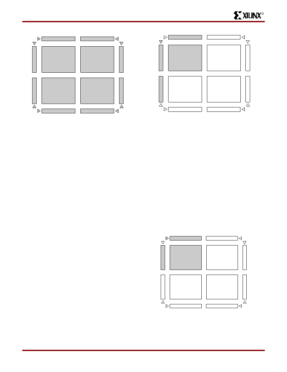
Figure 36: Any BUFGLS (GCK1 - GCK8) Can
Drive Any or All Clock Inputs on the Device
16
25
3
8
4
7
CLB
I
O
B
I
O
B
I
O
B
I
O
B
IOB
X6751
Figure 37: Left and Right BUFGEs Can Drive Any or
All Clock Inputs in Same Quadrant or Edge (GCK1 is
shown. GCK2, GCK5 and GCK6 are similar.)
16
25
3
8
4
7
CLB
I
O
B
I
O
B
I
O
B
I
O
B
IOB
X6747
Figure 38: Top and Bottom BUFGEs Can Drive Any
or All Clock Inputs in Same Quadrant (GCK8 is
shown. GCK3, GCK4 and GCK7 are similar.)
Product Obsolete or Under Obsolescence
相关PDF资料 |
PDF描述 |
|---|---|
| IDT7016L25J8 | IC SRAM 144KBIT 25NS 68PLCC |
| FMM36DRKI-S13 | CONN EDGECARD 72POS .156 EXTEND |
| MPC745CVT350LE | MCU HIP4DP 350MHZ 255-PBGA |
| MPC745CPX350LE | MCU HIP4DP 350MHZ 255-PBGA |
| MPC745BVT350LE | IC MPU PPC 350MHZ 255-FCPBGA |
相关代理商/技术参数 |
参数描述 |
|---|---|
| XC4036XL-2HQ304C | 功能描述:IC FPGA C-TEMP 3.3V 2SPD 304HQFP RoHS:否 类别:集成电路 (IC) >> 嵌入式 - FPGA(现场可编程门阵列) 系列:XC4000E/X 标准包装:1 系列:Kintex-7 LAB/CLB数:25475 逻辑元件/单元数:326080 RAM 位总计:16404480 输入/输出数:350 门数:- 电源电压:0.97 V ~ 1.03 V 安装类型:表面贴装 工作温度:0°C ~ 85°C 封装/外壳:900-BBGA,FCBGA 供应商设备封装:900-FCBGA(31x31) 其它名称:122-1789 |
| XC4036XL-2HQ304I | 功能描述:IC FPGA I-TEMP 3.3V 2SPD 304HQFP RoHS:否 类别:集成电路 (IC) >> 嵌入式 - FPGA(现场可编程门阵列) 系列:XC4000E/X 标准包装:1 系列:Kintex-7 LAB/CLB数:25475 逻辑元件/单元数:326080 RAM 位总计:16404480 输入/输出数:350 门数:- 电源电压:0.97 V ~ 1.03 V 安装类型:表面贴装 工作温度:0°C ~ 85°C 封装/外壳:900-BBGA,FCBGA 供应商设备封装:900-FCBGA(31x31) 其它名称:122-1789 |
| XC4036XL-3BG352C | 功能描述:IC FPGA C-TEMP 3.3V 3SPD 352MBGA RoHS:否 类别:集成电路 (IC) >> 嵌入式 - FPGA(现场可编程门阵列) 系列:XC4000E/X 标准包装:1 系列:Kintex-7 LAB/CLB数:25475 逻辑元件/单元数:326080 RAM 位总计:16404480 输入/输出数:350 门数:- 电源电压:0.97 V ~ 1.03 V 安装类型:表面贴装 工作温度:0°C ~ 85°C 封装/外壳:900-BBGA,FCBGA 供应商设备封装:900-FCBGA(31x31) 其它名称:122-1789 |
| XC4036XL-3BG352I | 功能描述:IC FPGA I-TEMP 3.3V 3SPD 352MBGA RoHS:否 类别:集成电路 (IC) >> 嵌入式 - FPGA(现场可编程门阵列) 系列:XC4000E/X 标准包装:1 系列:Kintex-7 LAB/CLB数:25475 逻辑元件/单元数:326080 RAM 位总计:16404480 输入/输出数:350 门数:- 电源电压:0.97 V ~ 1.03 V 安装类型:表面贴装 工作温度:0°C ~ 85°C 封装/外壳:900-BBGA,FCBGA 供应商设备封装:900-FCBGA(31x31) 其它名称:122-1789 |
| XC4036XL-3BG432C | 功能描述:IC FPGA C-TEMP 3.3V 3SPD 432MBGA RoHS:否 类别:集成电路 (IC) >> 嵌入式 - FPGA(现场可编程门阵列) 系列:XC4000E/X 标准包装:1 系列:Kintex-7 LAB/CLB数:25475 逻辑元件/单元数:326080 RAM 位总计:16404480 输入/输出数:350 门数:- 电源电压:0.97 V ~ 1.03 V 安装类型:表面贴装 工作温度:0°C ~ 85°C 封装/外壳:900-BBGA,FCBGA 供应商设备封装:900-FCBGA(31x31) 其它名称:122-1789 |
发布紧急采购,3分钟左右您将得到回复。