- 您现在的位置:买卖IC网 > PDF目录205934 > XC5204-6PQ208C (Xilinx, Inc.) Field Programmable Gate Arrays PDF资料下载
参数资料
| 型号: | XC5204-6PQ208C |
| 厂商: | Xilinx, Inc. |
| 英文描述: | Field Programmable Gate Arrays |
| 中文描述: | 现场可编程门阵列 |
| 文件页数: | 11/73页 |
| 文件大小: | 598K |
| 代理商: | XC5204-6PQ208C |
第1页第2页第3页第4页第5页第6页第7页第8页第9页第10页当前第11页第12页第13页第14页第15页第16页第17页第18页第19页第20页第21页第22页第23页第24页第25页第26页第27页第28页第29页第30页第31页第32页第33页第34页第35页第36页第37页第38页第39页第40页第41页第42页第43页第44页第45页第46页第47页第48页第49页第50页第51页第52页第53页第54页第55页第56页第57页第58页第59页第60页第61页第62页第63页第64页第65页第66页第67页第68页第69页第70页第71页第72页第73页
R
November 5, 1998 (Version 5.2)
7-101
XC5200 Series Field Programmable Gate Arrays
7
Even if the boundary scan symbol is used in a schematic,
the input pins TMS, TCK, and TDI can still be used as
inputs to be routed to internal logic. Care must be taken not
to force the chip into an undesired boundary scan state by
inadvertently applying boundary scan input patterns to
these pins. The simplest way to prevent this is to keep
TMS High, and then apply whatever signal is desired to TDI
and TCK.
Avoiding Inadvertent Boundary Scan
If TMS or TCK is used as user I/O, care must be taken to
ensure that at least one of these pins is held constant dur-
ing configuration. In some applications, a situation may
occur where TMS or TCK is driven during configuration.
This may cause the device to go into boundary scan mode
and disrupt the configuration process.
To prevent activation of boundary scan during configura-
tion, do either of the following:
TMS: Tie High to put the Test Access Port controller
in a benign RESET state
TCK: Tie High or Low—do not toggle this clock input.
For more information regarding boundary scan, refer to the
Xilinx Application Note XAPP 017, “
Boundary Scan in
XC4000 and XC5200 Devices.“
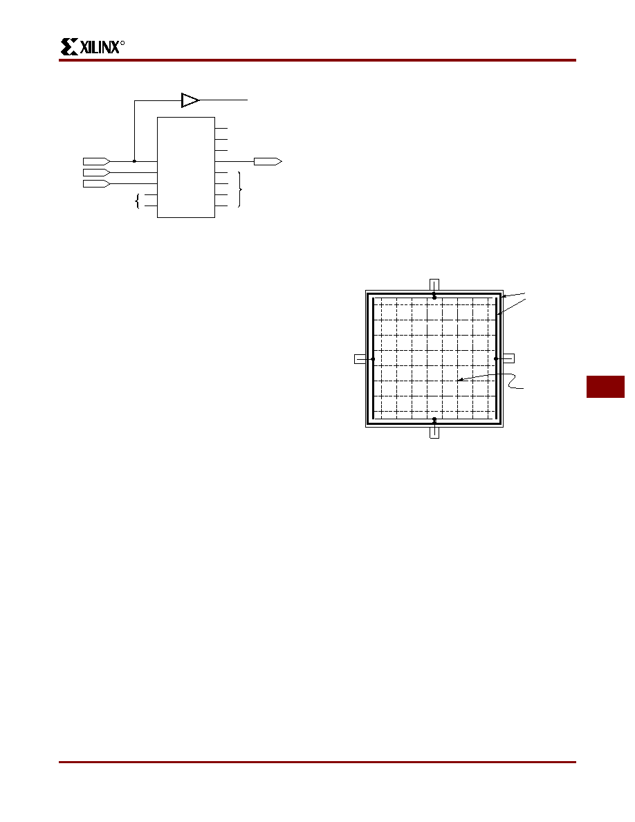
Power Distribution
Power for the FPGA is distributed through a grid to achieve
high noise immunity and isolation between logic and I/O.
Inside the FPGA, a dedicated Vcc and Ground ring sur-
rounding the logic array provides power to the I/O drivers,
as shown in Figure 21. An independent matrix of Vcc and
Ground lines supplies the interior logic of the device.
This power distribution grid provides a stable supply and
ground for all internal logic, providing the external package
power pins are all connected and appropriately decoupled.
Typically, a 0.1
F capacitor connected near the Vcc and
Ground pins of the package will provide adequate decou-
pling.
Output buffers capable of driving/sinking the specified 8 mA
loads under specified worst-case conditions may be capa-
ble of driving/sinking up to 10 times as much current under
best case conditions.
Noise can be reduced by minimizing external load capaci-
tance and reducing simultaneous output transitions in the
same direction. It may also be beneficial to locate heavily
loaded output buffers near the Ground pads. The I/O Block
output buffers have a slew-rate limited mode (default)
which should be used where output rise and fall times are
not speed-critical.
Pin Descriptions
There are three types of pins in the XC5200-Series
devices:
Permanently dedicated pins
User I/O pins that can have special functions
Unrestricted user-programmable I/O pins.
Before and during configuration, all outputs not used for the
configuration process are 3-stated and pulled high with a
20 k
- 100 k pull-up resistor.
After configuration, if an IOB is unused it is configured as
an input with a 20 k
- 100 k pull-up resistor.
Device pins for XC5200-Series devices are described in
Table 9. Pin functions during configuration for each of the
seven configuration modes are summarized in “Pin Func-
TDI
TMS
TCK
TDO1
TDO2
TDO
DRCK
IDLE
SEL1
SEL2
RESET
UPDATE
SHIFT
BSCAN
To User
Logic
IBUF
Optional
From
User Logic
To User
Logic
X9000
Figure 20: Boundary Scan Schematic Example
GND
Ground and
Vcc Ring for
I/O Drivers
Vcc
GND
Vcc
Logic
Power Grid
X5422
Figure 21: XC5200-Series Power Distribution
相关PDF资料 |
PDF描述 |
|---|---|
| XC5204-6PQ240C | Field Programmable Gate Arrays |
| XC5204-6TQ176C | Field Programmable Gate Arrays |
| XC5204-6VQ64C | Field Programmable Gate Arrays |
| XC5204-3TQ144C | Field Programmable Gate Arrays |
| XC5204-3VQ100C | Field Programmable Gate Arrays |
相关代理商/技术参数 |
参数描述 |
|---|---|
| XC5204-6PQ240C | 制造商:XILINX 制造商全称:XILINX 功能描述:Field Programmable Gate Arrays |
| XC5204-6PQG160C | 制造商:Xilinx 功能描述:XC5204-6PQG160C, FPGA XC5200 FAMILY 6K GATES 480 CELLS - Trays 制造商:Xilinx 功能描述:Xilinx XC5204-6PQG160C, FPGA XC5200 Family 6K Gates 480 Cells 83MHz 0.5um (CMOS) Technology 5V 160-Pin PQFP |
| XC5204-6TQ144C | 功能描述:IC FPGA 120 CLB'S 144-TQFP RoHS:否 类别:集成电路 (IC) >> 嵌入式 - FPGA(现场可编程门阵列) 系列:XC5200 产品变化通告:XC4000(E,L) Discontinuation 01/April/2002 标准包装:24 系列:XC4000E/X LAB/CLB数:100 逻辑元件/单元数:238 RAM 位总计:3200 输入/输出数:80 门数:3000 电源电压:4.5 V ~ 5.5 V 安装类型:表面贴装 工作温度:-40°C ~ 100°C 封装/外壳:120-BCBGA 供应商设备封装:120-CPGA(34.55x34.55) |
| XC5204-6TQ144I | 制造商:Xilinx 功能描述: |
| XC5204-6TQ176C | 制造商:XILINX 制造商全称:XILINX 功能描述:Field Programmable Gate Arrays |
发布紧急采购,3分钟左右您将得到回复。