- 您现在的位置:买卖IC网 > PDF目录205934 > XC5204-6TQ176C (Xilinx, Inc.) Field Programmable Gate Arrays PDF资料下载
参数资料
| 型号: | XC5204-6TQ176C |
| 厂商: | Xilinx, Inc. |
| 英文描述: | Field Programmable Gate Arrays |
| 中文描述: | 现场可编程门阵列 |
| 文件页数: | 45/73页 |
| 文件大小: | 598K |
| 代理商: | XC5204-6TQ176C |
第1页第2页第3页第4页第5页第6页第7页第8页第9页第10页第11页第12页第13页第14页第15页第16页第17页第18页第19页第20页第21页第22页第23页第24页第25页第26页第27页第28页第29页第30页第31页第32页第33页第34页第35页第36页第37页第38页第39页第40页第41页第42页第43页第44页当前第45页第46页第47页第48页第49页第50页第51页第52页第53页第54页第55页第56页第57页第58页第59页第60页第61页第62页第63页第64页第65页第66页第67页第68页第69页第70页第71页第72页第73页
R
November 5, 1998 (Version 5.2)
7-87
XC5200 Series Field Programmable Gate Arrays
7
single-length lines, double-length lines, and Longlines all
routed through the GRM. The direct connects, LIM, and
logic-cell
feedthrough
are
contained
within
each
Versa-Block. Throughout the XC5200 interconnect, an effi-
cient multiplexing scheme, in combination with three layer
metal (TLM), was used to improve the overall efficiency of
silicon usage.
Performance Overview
The XC5200 family has been benchmarked with many
designs running synchronous clock rates beyond 66 MHz.
The performance of any design depends on the circuit to be
implemented, and the delay through the combinatorial and
sequential logic elements, plus the delay in the intercon-
nect routing. A rough estimate of timing can be made by
assuming 3-6 ns per logic level, which includes direct-con-
nect routing delays, depending on speed grade. More
accurate estimations can be made using the information in
the Switching Characteristic Guideline section.
Taking Advantage of Reconfiguration
FPGA devices can be reconfigured to change logic function
while resident in the system. This capability gives the sys-
tem designer a new degree of freedom not available with
any other type of logic.
Hardware can be changed as easily as software. Design
updates or modifications are easy, and can be made to
products already in the field. An FPGA can even be recon-
figured dynamically to perform different functions at differ-
ent times.
Reconfigurable logic can be used to implement system
self-diagnostics, create systems capable of being reconfig-
ured for different environments or operations, or implement
multi-purpose hardware for a given application. As an
added benefit, using reconfigurable FPGA devices simpli-
fies hardware design and debugging and shortens product
time-to-market.
Detailed Functional Description
Configurable Logic Blocks (CLBs)
Figure 4 shows the logic in the XC5200 CLB, which con-
sists of four Logic Cells (LC[3:0]). Each Logic Cell consists
of an independent 4-input Lookup Table (LUT), and a
D-Type flip-flop or latch with common clock, clock enable,
and clear, but individually selectable clock polarity. Addi-
tional logic features provided in the CLB are:
An independent 5-input LUT by combining two 4-input
LUTs.
High-speed carry propagate logic.
High-speed pattern decoding.
High-speed direct connection to flip-flop D-inputs.
Individual selection of either a transparent,
level-sensitive latch or a D flip-flop.
Four 3-state buffers with a shared Output Enable.
5-Input Functions
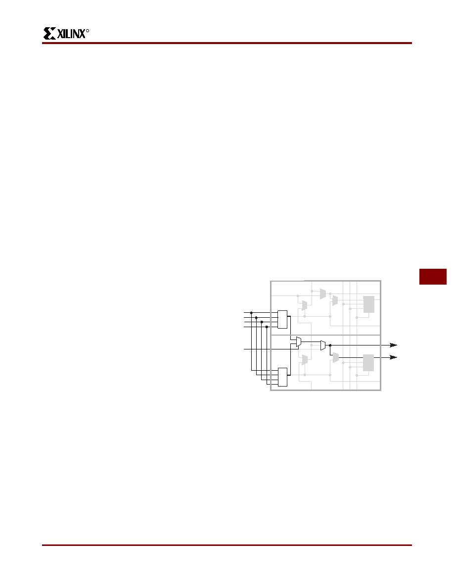
Figure 5 illustrates how the outputs from the LUTs from
LC0 and LC1 can be combined with a 2:1 multiplexer
(F5_MUX) to provide a 5-input function. The outputs from
the LUTs of LC2 and LC3 can be similarly combined.
Figure 5: Two LUTs in Parallel Combined to Create a
5-input Function
out
Q
Qout
DO
Q
D
FD
X
FD
CO
DI
X
CLR
LC0
CK
CE
5-Input Function
D
DO
F5_MUX
DI
F
F4
F3
F2
F1
F4
F3
F2
F1
I1
I2
I3
I4
I5
CI
F
LC1
X5710
相关PDF资料 |
PDF描述 |
|---|---|
| XC5204-6VQ64C | Field Programmable Gate Arrays |
| XC5204-3TQ144C | Field Programmable Gate Arrays |
| XC5204-3VQ100C | Field Programmable Gate Arrays |
| XC5204-4PC84C | Field Programmable Gate Arrays |
| XC5204-6PC84C | Field Programmable Gate Arrays |
相关代理商/技术参数 |
参数描述 |
|---|---|
| XC5204-6VQ100C | 功能描述:IC FPGA 120 CLB'S 100-VQFP RoHS:否 类别:集成电路 (IC) >> 嵌入式 - FPGA(现场可编程门阵列) 系列:XC5200 产品变化通告:XC4000(E,L) Discontinuation 01/April/2002 标准包装:24 系列:XC4000E/X LAB/CLB数:100 逻辑元件/单元数:238 RAM 位总计:3200 输入/输出数:80 门数:3000 电源电压:4.5 V ~ 5.5 V 安装类型:表面贴装 工作温度:-40°C ~ 100°C 封装/外壳:120-BCBGA 供应商设备封装:120-CPGA(34.55x34.55) |
| XC5204-6VQ100I | 制造商:Xilinx 功能描述: |
| XC5204-6VQ64C | 制造商:XILINX 制造商全称:XILINX 功能描述:Field Programmable Gate Arrays |
| XC5204-6VQG100C | 制造商:Xilinx 功能描述:FPGA XC5200 6K GATES 480 CELLS 83MHZ COMM 0.5UM 5V 100VTQFP - Trays 制造商:Xilinx 功能描述:Xilinx XC5204-6VQG100C FPGA |
| XC5206 | 制造商:XILINX 制造商全称:XILINX 功能描述:Field Programmable Gate Arrays |
发布紧急采购,3分钟左右您将得到回复。