参数资料
| 型号: | XC5VLX220T-2FFG1738C |
| 厂商: | Xilinx Inc |
| 文件页数: | 1/91页 |
| 文件大小: | 0K |
| 描述: | IC FPGA VIRTEX-5 220K 1738FBGA |
| 标准包装: | 1 |
| 系列: | Virtex®-5 LXT |
| LAB/CLB数: | 17280 |
| 逻辑元件/单元数: | 221184 |
| RAM 位总计: | 7815168 |
| 输入/输出数: | 680 |
| 电源电压: | 0.95 V ~ 1.05 V |
| 安装类型: | 表面贴装 |
| 工作温度: | 0°C ~ 85°C |
| 封装/外壳: | 1738-BBGA,FCBGA |
| 供应商设备封装: | 1738-FCBGA |
| 配用: | 568-5088-ND - BOARD DEMO DAC1408D750 |
当前第1页第2页第3页第4页第5页第6页第7页第8页第9页第10页第11页第12页第13页第14页第15页第16页第17页第18页第19页第20页第21页第22页第23页第24页第25页第26页第27页第28页第29页第30页第31页第32页第33页第34页第35页第36页第37页第38页第39页第40页第41页第42页第43页第44页第45页第46页第47页第48页第49页第50页第51页第52页第53页第54页第55页第56页第57页第58页第59页第60页第61页第62页第63页第64页第65页第66页第67页第68页第69页第70页第71页第72页第73页第74页第75页第76页第77页第78页第79页第80页第81页第82页第83页第84页第85页第86页第87页第88页第89页第90页第91页

DS202 (v5.3) May 5, 2010
Product Specification
1
2006–2010 Xilinx, Inc. XILINX, the Xilinx logo, Virtex, Spartan, ISE, and other designated brands included herein are trademarks of Xilinx in the United States and other
countries. PowerPC is a trademark of IBM Corp. and is used under license. PCI, PCI Express, PCIe, and PCI-X are trademarks of PCI-SIG. All other trademarks are the property
of their respective owners.
Virtex-5 FPGA Electrical Characteristics
Virtex-5 FPGAs are available in -3, -2, -1 speed grades,
with -3 having the highest performance. Virtex-5 FPGA DC
and AC characteristics are specified for both commercial
and industrial grades. Except the operating temperature
range or unless otherwise noted, all the DC and AC
electrical parameters are the same for a particular speed
grade (that is, the timing characteristics of a -1 speed grade
industrial device are the same as for a -1 speed grade
commercial device). However, only selected speed grades
and/or devices might be available in the industrial range.
All supply voltage and junction temperature specifications
are representative of worst-case conditions. The
parameters included are common to popular designs and
typical applications.
This Virtex-5 FPGA data sheet, part of an overall set of
documentation on the Virtex-5 family of FPGAs, is available
on the Xilinx website:
All specifications are subject to change without notice.
Virtex-5 FPGA DC Characteristics
0
Virtex-5 FPGA Data Sheet:
DC and Switching Characteristics
DS202 (v5.3) May 5, 2010
00
Product Specification
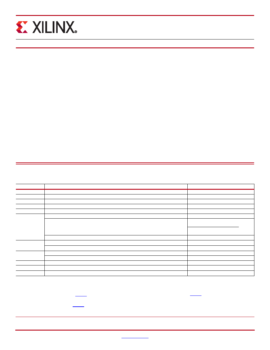
Table 1: Absolute Maximum Ratings
Symbol
Description
Units
VCCINT
Internal supply voltage relative to GND
–0.5 to 1.1
V
VCCAUX
Auxiliary supply voltage relative to GND
–0.5 to 3.0
V
VCCO
Output drivers supply voltage relative to GND
–0.5 to 3.75
V
VBATT
Key memory battery backup supply
–0.5 to 4.05
V
VREF
Input reference voltage
–0.5 to 3.75
V
VIN(3)
3.3V I/O input voltage relative to GND(4) (user and dedicated I/Os)
–0.75 to 4.05
V
3.3V I/O input voltage relative to GND (restricted to maximum of 100 user I/Os)(5)
–0.95 to 4.4
(Commercial Temperature)
V
–0.85 to 4.3
(Industrial Temperature)
2.5V or below I/O input voltage relative to GND (user and dedicated I/Os)
–0.75 to VCCO + 0.5
V
IIN
Current applied to an I/O pin, powered or unpowered
±100
mA
Total current applied to all I/O pins, powered or unpowered
±100
mA
VTS
Voltage applied to 3-state 3.3V output(4) (user and dedicated I/Os)
–0.75 to 4.05
V
Voltage applied to 3-state 2.5V or below output (user and dedicated I/Os)
–0.75 to VCCO + 0.5
V
TSTG
Storage temperature (ambient)
–65 to 150
°C
TSOL
Maximum soldering temperature(2)
+220
°C
TJ
Maximum junction temperature(2)
+125
°C
Notes:
1.
Stresses beyond those listed under Absolute Maximum Ratings might cause permanent damage to the device. These are stress ratings only, and
functional operation of the device at these or any other conditions beyond those listed under Operating Conditions is not implied. Exposure to Absolute
Maximum Ratings conditions for extended periods of time might affect device reliability.
2.
For soldering guidelines, refer to UG112: Device Package User Guide. For thermal considerations, refer to UG195: Virtex-5 FPGA Packaging and
Pinout Specification on the Xilinx website.
3.
3.3V I/O absolute maximum limit applied to DC and AC signals.
4.
For 3.3V I/O operation, refer to UG190: Virtex-5 FPGA User Guide, Chapter 6, 3.3V I/O Design Guidelines.
5.
For more flexibility in specific designs, a maximum of 100 user I/Os can be stressed beyond the normal specification for no more than 20% of a data period.
相关PDF资料 |
PDF描述 |
|---|---|
| XC5VLX155T-2FF1738I | IC FPGA VIRTEX-5LXT 1738FFBGA |
| EMC65DRAI | CONN EDGECARD 130PS R/A .100 SLD |
| XC4VLX200-10FFG1513C | IC FPGA VIRTEX-4LX 200K 1513FBGA |
| ABC65DRYS | CONN EDGECARD 130PS .100 DIP SLD |
| ACB64DHAN | CONN EDGECARD 128PS R/A .050 DIP |
相关代理商/技术参数 |
参数描述 |
|---|---|
| XC5VLX220T-2FFG1738CES | 制造商:Xilinx 功能描述: |
| XC5VLX220T-2FFG1738I | 功能描述:IC FPGA VIRTEX-5 220K 1738FBGA RoHS:是 类别:集成电路 (IC) >> 嵌入式 - FPGA(现场可编程门阵列) 系列:Virtex®-5 LXT 产品变化通告:XC4000(E,L) Discontinuation 01/April/2002 标准包装:24 系列:XC4000E/X LAB/CLB数:100 逻辑元件/单元数:238 RAM 位总计:3200 输入/输出数:80 门数:3000 电源电压:4.5 V ~ 5.5 V 安装类型:表面贴装 工作温度:-40°C ~ 100°C 封装/外壳:120-BCBGA 供应商设备封装:120-CPGA(34.55x34.55) |
| XC5VLX30 | 制造商:XILINX 制造商全称:XILINX 功能描述:Virtex-5 Family Overview |
| XC5VLX30-1FF324C | 功能描述:IC FPGA VIRTEX-5 30K 324FBGA RoHS:否 类别:集成电路 (IC) >> 嵌入式 - FPGA(现场可编程门阵列) 系列:Virtex®-5 LX 产品变化通告:Step Intro and Pkg Change 11/March/2008 标准包装:1 系列:Virtex®-5 SXT LAB/CLB数:4080 逻辑元件/单元数:52224 RAM 位总计:4866048 输入/输出数:480 门数:- 电源电压:0.95 V ~ 1.05 V 安装类型:表面贴装 工作温度:-40°C ~ 100°C 封装/外壳:1136-BBGA,FCBGA 供应商设备封装:1136-FCBGA 配用:568-5088-ND - BOARD DEMO DAC1408D750122-1796-ND - EVALUATION PLATFORM VIRTEX-5 |
| XC5VLX30-1FF324CES | 制造商:Xilinx 功能描述: |
发布紧急采购,3分钟左右您将得到回复。