- 您现在的位置:买卖IC网 > PDF目录14928 > XC9119D10AMR-G (Torex Semiconductor Ltd)IC REG BOOST ADJ 0.31A SOT25-5 PDF资料下载
参数资料
| 型号: | XC9119D10AMR-G |
| 厂商: | Torex Semiconductor Ltd |
| 文件页数: | 5/18页 |
| 文件大小: | 0K |
| 描述: | IC REG BOOST ADJ 0.31A SOT25-5 |
| 标准包装: | 1 |
| 类型: | 升压(升压) |
| 输出类型: | 可调式 |
| 输出数: | 1 |
| 输出电压: | 可调至 19.5V |
| 输入电压: | 2.5 V ~ 6 V |
| 频率 - 开关: | 1MHz |
| 电流 - 输出: | 310mA |
| 同步整流器: | 无 |
| 工作温度: | -40°C ~ 85°C |
| 安装类型: | 表面贴装 |
| 封装/外壳: | SC-74A,SOT-753 |
| 包装: | 标准包装 |
| 供应商设备封装: | SOT-25 |
| 其它名称: | 893-1165-6 |
�� �
�
�XC9119D10A�
�Series�
�■� OPERATIONAL� EXPLANATION�
�The� XC9119D10A� series� consists� of� a� reference� voltage� source,� ramp� wave� circuit,� error� amplifier,� PWM� comparator,� phase�
�compensation� circuit,� driver� transistor,� current� limiter� circuit� and� others.� The� series� ICs� compare,� using� the� error� amplifier,� the�
�voltage� of� the� internal� reference� voltage� source� with� the� feedback� voltage� from� the� FB� pin.� Phase� compensation� is� performed�
�on� the� resulting� error� amplifier� output,� to� input� a� signal� to� the� PWM� comparator� to� determine� the� turn-on� time� during� switching.�
�The� PWM� comparator� compares,� in� terms� of� voltage� level,� the� signal� from� the� error� amplifier� with� the� ramp� wave� from� the� ramp�
�wave� circuit,� and� delivers� the� resulting� output� to� the� buffer� drive� circuit� to� cause� the� Lx� pin� to� output� a� switching� duty� cycle.�
�This� process� is� continuously� performed� to� ensure� stable� output� voltage.� The� current� feedback� circuit� detects� the� N-channel�
�MOS� driver� transistor's� current� for� each� switching� operation,� and� modulates� the� error� amplifier� output� signal� to� provide� multiple�
�feedback� signals.� This� enables� a� stable� feedback� loop� even� when� a� low� ESR� capacitor,� such� as� a� ceramic� capacitor,� is� used,�
�ensuring� stable� output� voltage.�
�<Reference� Voltage� Source>�
�The� reference� voltage� source� provides� the� reference� voltage� to� ensure� stable� output� voltage� of� the� IC.�
�<Ramp� Wave� Circuit>�
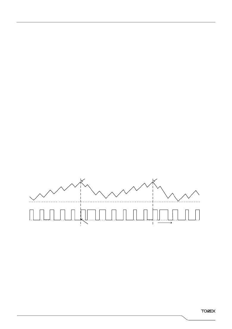
�The� ramp� wave� circuit� determines� switching� frequency.� The� 1MHz� (TYP.)� of� frequency� is� fixed� internally.� Clock� pulses�
�generated� in� this� circuit� are� used� to� produce� ramp� waveforms� needed� for� PWM� operation.�
�<Error� Amplifier>�
�The� error� amplifier� is� designed� to� monitor� output� voltage.� The� amplifier� compares� the� reference� voltage� with� the� FB� pin�
�voltage.� When� a� voltage� lower� than� the� reference� voltage� is� fed� back,� the� output� voltage� of� the� error� amplifier� increases.�
�Gain� and� frequency� characteristics� of� the� error� amplifier� output� are� fixed� internally� as� an� optimize� signal.�
�<Current� Limit� >�
�The� current� limit� circuit� of� the� XC9119D10A� series� monitors� the� current� flowing� through� the� N-channel� MOS� driver�
�transistor� connected� to� the� Lx� pin,� and� features� a� combination� of� the� constant-current� type� current� limit� mode� and� the�
�duty� cycle� limit� of� the� next� pulse.�
�①� When� the� driver� current� is� greater� than� a� specific� level,� the� constant-current� type� current� limit� function� operates� to� turn�
�off� the� pulses� from� the� Lx� pin� at� any� given� timing.�
�②� The� IC� controls� the� next� pulse� to� be� smaller� than� the� first� pulse.�
�IL�
�Lx�
�Current� Limit�
�1�
�The� current� will� be� off� when� the� coil� current�
�Current� Limit�
�2�
�Limit� some� duty� pulses� after� the� limit.�
�reaches� the� value� of� the� constant� current� limit.�
�<CE� Pin� Function>�
�The� operation� of� the� XC9119D10A� series� will� enter� into� the� shut� down� mode� when� a� low� level� signal� is� input� to� the� CE�
�pin.� During� the� shut� down� mode,� the� supply� current� is� 0� μ� A� (TYP.),� with� high� impedance� at� the� Lx� pin.� The� IC� starts� its�
�operation� with� a� high� level� signal� to� the� CE� pin.� The� input� to� the� CE� pin� is� a� CMOS� input� and� the� sink� current� is� 0� μ� A�
�(TYP.).� The� hysteresis� between� the� chip� enable� and� the� chip� disable� is� 50mV� (TYP.).�
�<Soft-Start� Time>�
�Soft-start� function� operates� when� capacitors� and� resistors� are� connected� to� the� CE/SS� pin.� With� the� Vref� voltage� limited�
�by� the� CE/SS� pin� start-up� voltage� and� applying� the� input� to� the� error� amps,� the� operation� maintains� a� balance� between�
�the� two� inputs� of� the� error� amps.� and� controls� the� Lx� pin’s� ON� time� so� that� it� doesn’t� increase� more� than� is� necessary.�
�Depending� of� current� limit� function,� load� current,� step-up� ratio,� and� external� components,� the� IC� takes� about� 500uS� to� 5mS�
�to� attain� the� setting� voltage� after� applying� the� CE� ‘H’� voltage� even� though� the� R� SS� is� 0� Ω� and� a� soft� start� capacitor� C� SS� is� not�
�connected.� (For� a� numerical� constant,� please� refer� to� Note� on� Use.)� For� longer� soft-start� time,� please� connect� R� SS� and� C� SS� .�
�Soft-start� function� operates� while� the� CE� pin� voltage� is� between� 0V� to� around� 1.9V.� Please� be� noted� that� if� the� CE/SS� pin� voltage�
�does� not� start� from� 0V� but� is� in� intermediate� potential� when� the� power� is� turned� on� etc.,� soft� start� function� may� lose� an� effect� and�
�that� will� cause� a� high� inrush� current� and� ripple� voltage.�
�5/18�
�相关PDF资料 |
PDF描述 |
|---|---|
| VE-2TZ-EX-F2 | CONVERTER MOD DC/DC 2V 30W |
| XC6372A551PR-G | IC REG BOOST 5.5V 0.1A SOT89 |
| GBB45DHRN | CONN CARD EXTEND 90POS .050" SLD |
| XC6372A331PR-G | IC REG BOOST 3.3V 0.1A SOT89 |
| H5BXT-10103-B7-ND | JUMPER-H2728TR/C2065B/X 3" |
相关代理商/技术参数 |
参数描述 |
|---|---|
| XC9128B45CAR | 制造商:Torex Semiconductor LTD 功能描述: |
| XC9128B45CAR-G | 功能描述:IC REG BST SYNC ADJ 1.2A MSOP10 RoHS:是 类别:集成电路 (IC) >> PMIC - 稳压器 - DC DC 开关稳压器 系列:- 标准包装:500 系列:- 类型:切换式电容器(充电泵),反相 输出类型:固定 输出数:1 输出电压:-3V 输入电压:2.3 V ~ 5.5 V PWM 型:Burst Mode? 频率 - 开关:900kHz 电流 - 输出:100mA 同步整流器:无 工作温度:-40°C ~ 85°C 安装类型:表面贴装 封装/外壳:SOT-23-6 细型,TSOT-23-6 包装:带卷 (TR) 供应商设备封装:TSOT-23-6 其它名称:LTC1983ES6-3#TRMTR |
| XC9128B45CDR | 制造商:Torex Semiconductor LTD 功能描述: |
| XC9128B45CDR-G | 制造商:Torex Semiconductor LTD 功能描述: |
| XC9128B45CSRN | 制造商:Torex Semiconductor LTD 功能描述: |
发布紧急采购,3分钟左右您将得到回复。