- 您现在的位置:买卖IC网 > PDF目录19553 > XC95288XV-10TQ144C (Xilinx Inc)IC CPLD 2.5V ISP 144-TQFP PDF资料下载
参数资料
| 型号: | XC95288XV-10TQ144C |
| 厂商: | Xilinx Inc |
| 文件页数: | 9/14页 |
| 文件大小: | 0K |
| 描述: | IC CPLD 2.5V ISP 144-TQFP |
| 产品变化通告: | Product Discontinuation Notice 14/May/2007 |
| 标准包装: | 60 |
| 系列: | XC9500XV |
| 可编程类型: | 系统内可编程 |
| 最大延迟时间 tpd(1): | 10.0ns |
| 电压电源 - 内部: | 2.37 V ~ 2.62 V |
| 逻辑元件/逻辑块数目: | 16 |
| 宏单元数: | 288 |
| 门数: | 6400 |
| 输入/输出数: | 117 |
| 工作温度: | 0°C ~ 70°C |
| 安装类型: | 表面贴装 |
| 封装/外壳: | 144-LQFP |
| 供应商设备封装: | 144-TQFP(20x20) |
| 包装: | 托盘 |
| 其它名称: | XC95288XV10TQ144C |
XC95288XV High-Performance CPLD
4
DS050 (v3.0) June 25, 2007
Product Specification
R
Supported I/O Standards
The XC95288XV CPLD features both LVCMOS and LVTTL
I/O implementations. See Table 1 for I/O standard voltages.
The LVTTL I/O standard is a general purpose EIA/JEDEC
standard for 3.3V applications that use an LVTTL input
buffer and Push-Pull output buffer. The LVCMOS2 standard
is used in 2.5V applications.
XC9500XV CPLDs are also 1.8V I/O compatible. The
X25TO18 setting is provided for generating 1.8V compatible
outputs from a CPLD normally operating in a 2.5V environ-
ment. The ISE software automatically groups outputs with
matching IOSTANDARD settings into the same VCCIO bank
when no location constraints are specified. The default I/O
Standard for pads without IOSTANDARD attributes is
LVTTL for XC9500XV devices.
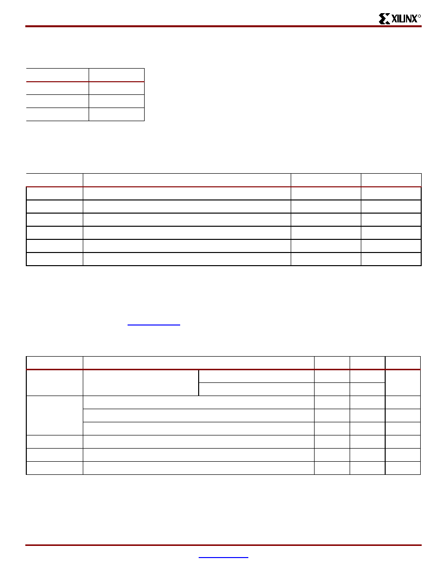
Absolute Maximum Ratings
Recommended Operation Conditions
Table 1: IOSTANDARD Options
IOSTANDARD
VCCIO
LVTTL
3.3V
LVCMOS2
2.5V
X25TO18
1.8V
Symbol
Description
Value
Units
VCC
Supply voltage relative to GND
–0.5 to 2.7
V
VCCIO
Supply voltage for output drivers
–0.5 to 3.6
V
VIN
Input voltage relative to GND(1)
–0.5 to 3.6
V
VTS
Voltage applied to 3-state output(1)
–0.5 to 3.6
V
TSTG
Storage temperature (ambient)
–65 to +150
oC
TJ
Junction temperature
+150
oC
Notes:
1.
Maximum DC undershoot below GND must be limited to either 0.5V or 10 mA, whichever is easier to achieve. During transitions, the
device pins may undershoot to –2.0V or overshoot to +3.6V, provided this over- or undershoot lasts less than 10 ns and with the
forcing current being limited to 200 mA.
2.
Stresses beyond those listed under Absolute Maximum Ratings may cause permanent damage to the device. These are stress
ratings only, and functional operation of the device at these or any other conditions beyond those listed under Operating Conditions
is not implied. Exposure to Absolute Maximum Ratings conditions for extended periods of time may affect device reliability.
3.
For solder specifications, see Xilinx Packaging.
Symbol
Parameter
Min
Max
Units
VCCINT
Supply voltage for internal logic
and input buffers
Commercial TA = 0oC to +70oC
2.37
2.62
V
Industrial TA = –40oC to +85oC
2.37
2.62
VCCIO
Supply voltage for output drivers for 3.3V operation
3.0
3.6
V
Supply voltage for output drivers for 2.5V operation
2.37
2.62
V
Supply voltage for output drivers for 1.8V operation
1.71
1.89
V
VIL
Low-level input voltage
0
0.8
V
VIH
High-level input voltage
1.7
3.6
V
VO
Output voltage
0
VCCIO
V
Product Obsolete/Under Obsolescence
相关PDF资料 |
PDF描述 |
|---|---|
| AP1084DL-13 | IC REG LDO ADJ 5A TO-252 |
| TPSB474M035R4000 | CAP TANT 0.47UF 35V 20% 1210 |
| A181M15X7RL5UAA | CAP CER 180PF 500V 20% X7R AXIAL |
| GEC08DRYN-S734 | CONN EDGECARD 16POS DIP .100 SLD |
| GEC05DREI | CONN EDGECARD 10POS .100 EYELET |
相关代理商/技术参数 |
参数描述 |
|---|---|
| XC95288XV-10TQ144I | 制造商:XILINX 制造商全称:XILINX 功能描述:High-Performance CPLD |
| XC95288XV-5CS280C | 制造商:XILINX 制造商全称:XILINX 功能描述:High-Performance CPLD |
| XC95288XV-5CS280I | 制造商:XILINX 制造商全称:XILINX 功能描述:High-Performance CPLD |
| XC95288XV-5FG256C | 制造商:XILINX 制造商全称:XILINX 功能描述:High-Performance CPLD |
| XC95288XV-5FG256I | 制造商:XILINX 制造商全称:XILINX 功能描述:High-Performance CPLD |
发布紧急采购,3分钟左右您将得到回复。