- 您现在的位置:买卖IC网 > PDF目录19497 > XC9572XL-10TQ100C (Xilinx Inc)IC CPLD 72 MCELL C-TEMP 100-TQFP PDF资料下载
参数资料
| 型号: | XC9572XL-10TQ100C |
| 厂商: | Xilinx Inc |
| 文件页数: | 4/10页 |
| 文件大小: | 0K |
| 描述: | IC CPLD 72 MCELL C-TEMP 100-TQFP |
| 标准包装: | 90 |
| 系列: | XC9500XL |
| 可编程类型: | 系统内可编程(最少 10,000 次编程/擦除循环) |
| 最大延迟时间 tpd(1): | 10.0ns |
| 电压电源 - 内部: | 3 V ~ 3.6 V |
| 逻辑元件/逻辑块数目: | 4 |
| 宏单元数: | 72 |
| 门数: | 1600 |
| 输入/输出数: | 72 |
| 工作温度: | 0°C ~ 70°C |
| 安装类型: | 表面贴装 |
| 封装/外壳: | 100-LQFP |
| 供应商设备封装: | 100-TQFP(14x14) |
| 包装: | 托盘 |
| 配用: | 122-1512-ND - KIT DESIGN CPLD W/BATT HOLDER |
| 其它名称: | 122-1264 XC9572XL-10TQ100C-ND |
XC9572XL High Performance CPLD
DS057 (v2.0) April 3, 2007
3
Product Specification
R
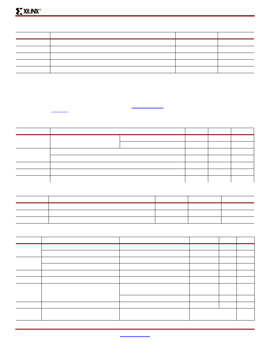
Absolute Maximum Ratings(2)
Recommended Operation Conditions
Quality and Reliability Characteristics
DC Characteristic Over Recommended Operating Conditions
Symbol
Description
Value
Units
VCC
Supply voltage relative to GND
–0.5 to 4.0
V
VIN
Input voltage relative to GND(1)
–0.5 to 5.5
V
VTS
Voltage applied to 3-state output(1)
–0.5 to 5.5
V
TSTG
Storage temperature (ambient)(3)
–65 to +150
oC
TJ
Junction temperature
+150
oC
Notes:
1.
Maximum DC undershoot below GND must be limited to either 0.5V or 10 mA, whichever is easier to achieve. During transitions, the
device pins may undershoot to –2.0 V or overshoot to +7.0V, provided this over- or undershoot lasts less than 10 ns and with the
forcing current being limited to 200 mA. External I/O voltage may not exceed VCCINT by 4.0V.
2.
Stresses beyond those listed under Absolute Maximum Ratings may cause permanent damage to the device. These are stress
ratings only, and functional operation of the device at these or any other conditions beyond those listed under Operating Conditions
is not implied. Exposure to Absolute Maximum Ratings conditions for extended periods of time may affect device reliability.
3.
For soldering guidelines and thermal considerations, see the Device Packaging information on the Xilinx website. For Pb-free
packages, see XAPP427.
Symbol
Parameter
Min
Max
Units
VCCINT
Supply voltage for internal logic
and input buffers
Commercial TA = 0oC to 70oC3.0
3.6
V
Industrial TA = –40oC to +85oC3.0
3.6
V
VCCIO
Supply voltage for output drivers for 3.3V operation
3.0
3.6
V
Supply voltage for output drivers for 2.5V operation
2.3
2.7
V
VIL
Low-level input voltage
0
0.80
V
VIH
High-level input voltage
2.0
5.5
V
VO
Output voltage
0
VCCIO
V
Symbol
Parameter
Min
Max
Units
TDR
Data Retention
20
-
Years
NPE
Program/Erase Cycles (Endurance)
10,000
-
Cycles
VESD
Electrostatic Discharge (ESD)
2,000
-
Volts
Symbol
Parameter
Test Conditions
Min
Max
Units
VOH
Output high voltage for 3.3V outputs
IOH = –4.0 mA
2.4
-
V
Output high voltage for 2.5V outputs
IOH = –500 μA90% VCCIO
-V
VOL
Output low voltage for 3.3V outputs
IOL = 8.0 mA
-
0.4
V
Output low voltage for 2.5V outputs
IOL = 500 μA-
0.4
V
IIL
Input leakage current
VCC = Max; VIN = GND or VCC
-±10
μA
IIH
I/O high-Z leakage current
VCC = Max; VIN = GND or VCC
-±10
μA
IIH
I/O high-Z leakage current
VCC = Max; VCCIO = Max;
VIN = GND or 3.6V
-±10
μA
VCC Min < VIN < 5.5V
-
±50
μA
CIN
I/O capacitance
VIN = GND; f = 1.0 MHz
-
10
pF
ICC
Operating supply current
(low power mode, active)
VIN = GND, No load; f = 1.0 MHz
20 (Typical)
mA
相关PDF资料 |
PDF描述 |
|---|---|
| EBC06DTBH | CONN EDGECARD 12POS R/A .100 SLD |
| RS-2405DZ | CONV DC/DC 2W 9-36VIN +/-05VOUT |
| MAX6641AUB96+ | IC TEMP MONITOR SMBUS 10UMAX |
| EEC07DREI | CONN EDGECARD 14POS .100 EYELET |
| ECC05DREH | CONN EDGECARD 10POS .100 EYELET |
相关代理商/技术参数 |
参数描述 |
|---|---|
| XC9572XL-10TQ100C0167 | 制造商:Xilinx 功能描述: |
| XC9572XL-10TQ100C0696 | 制造商:Xilinx 功能描述: |
| XC9572XL-10TQ100C0768 | 制造商:Xilinx 功能描述: |
| XC9572XL-10TQ100C0952 | 制造商:Xilinx 功能描述: |
| XC9572XL-10TQ100C0962 | 制造商:Xilinx 功能描述: |
发布紧急采购,3分钟左右您将得到回复。