- 您现在的位置:买卖IC网 > PDF目录19664 > XCR3384XL-7FG324C (Xilinx Inc)IC CPLD 3.3V ZERO PWR 324-FBGA PDF资料下载
参数资料
| 型号: | XCR3384XL-7FG324C |
| 厂商: | Xilinx Inc |
| 文件页数: | 9/12页 |
| 文件大小: | 0K |
| 描述: | IC CPLD 3.3V ZERO PWR 324-FBGA |
| 标准包装: | 60 |
| 系列: | CoolRunner XPLA3 |
| 可编程类型: | 系统内可编程(最少 1K 次编程/擦除循环) |
| 最大延迟时间 tpd(1): | 7.0ns |
| 电压电源 - 内部: | 3 V ~ 3.6 V |
| 逻辑元件/逻辑块数目: | 24 |
| 宏单元数: | 384 |
| 门数: | 9000 |
| 输入/输出数: | 220 |
| 工作温度: | 0°C ~ 70°C |
| 安装类型: | 表面贴装 |
| 封装/外壳: | 324-BBGA |
| 供应商设备封装: | 324-FBGA(23x23) |
| 包装: | 托盘 |
CoolRunner XPLA3 CPLD
6
DS012 (v2.5) May 26, 2009
Product Specification
R
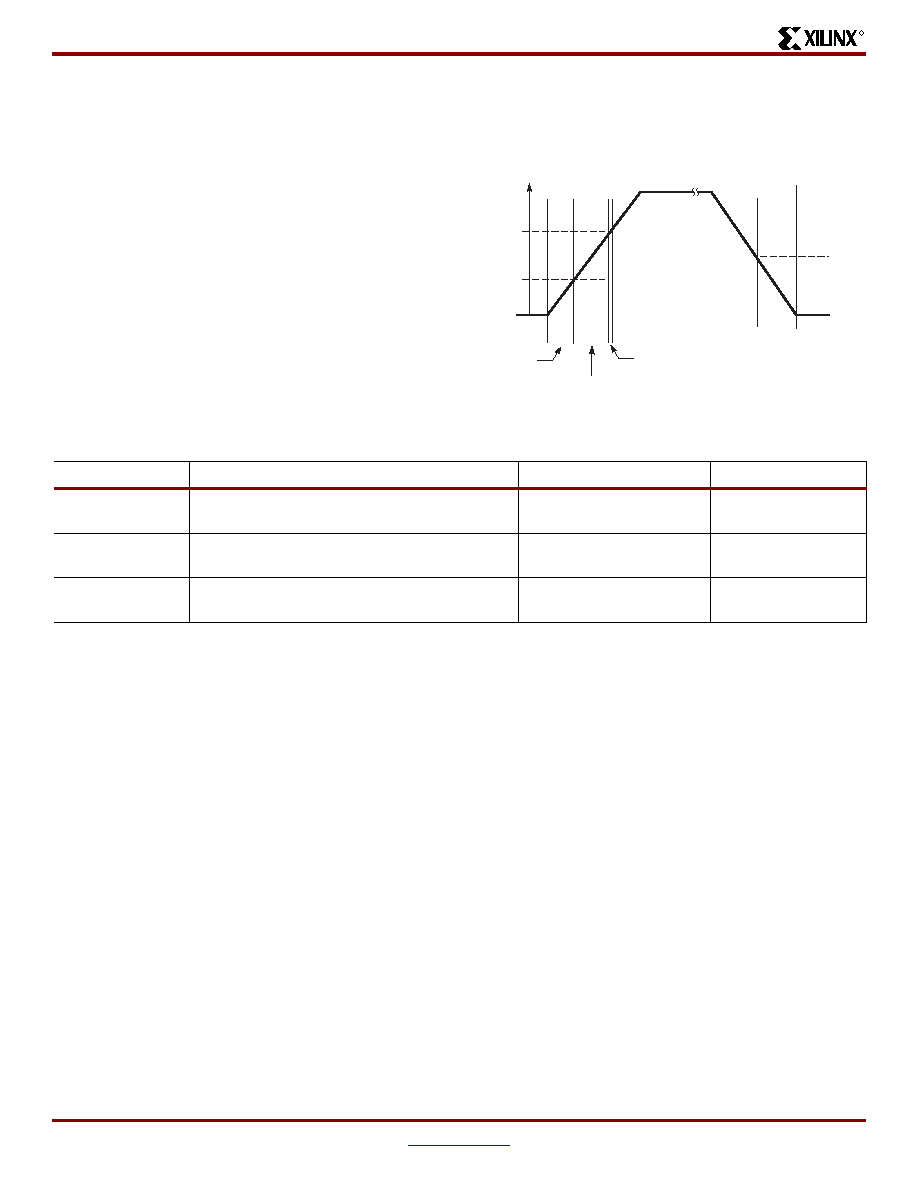
Power-Up Characteristics
During power-up, the CoolRunner XPLA3 device I/Os may
be undefined until VCC rises above 1.0V. This time period is
called the Subthreshold State, as transistors have not yet
fully been turned on. When VCC rises above 1.0V, the
device I/Os enter the Quiescent State, and I/Os are dis-
abled with weak pull-ups as shown in Table 3. When VCC
reaches the threshold of the User Operation State (approx-
imately 2.1V), user registers are initialized (typically within
200
μs) after which I/Os assume the behavior determined
by the user pattern, as shown in Figure 7.
If the device is in the erased state (before any user pattern
is programmed), the device outputs remain disabled with
weak pull-ups. The JTAG pins are enabled to allow the
device to be programmed at any time. All devices are
shipped in the erased state from the factory.
If the device is programmed, the device inputs and outputs
take on their configured states for normal operation.
Security
Designs can be secured during programming to prevent
pattern theft via readback. This security setting does not
protect readback of the Usercode/signature space, which is
often used for storing application serial numbers or revision
codes. The only way to clear the security setting is to com-
pletely erase the entire device.
Timing Model
The CoolRunner XPLA3 architecture follows a timing model
that allows deterministic timing in design and redesign. The
basic timing model is shown in Figure 8. There is a fast path
(TLOGI1) into the macrocell which is used if there is a single
product term. The TLOGI2 path is used for multiple product
term timing. For optimization of logic, the CoolRunner
XPLA3 CPLD architecture includes a Foldback NAND path
(TLOGI3). There is a fast input path to each macrocell if used
as an Input Register (TFIN). The CoolRunner XPLA3 archi-
tecture also includes universal control terms (TUDA) that can
be used for synchronization of the macrocell registers in dif-
ferent function blocks. There is slew rate control and output
enable control on a per macrocell basis.
Figure 7: Device Behavior During Power Up
V CC
No
Power
3.8 V
(Typ)
0V
No
Power
Quiescent
State
Quiescent
State
User Operation State
Initialization of User Registers
DS012_12_082707
2.1V
1.6V
(Typ)
Subthreshold
State
1.0V
Table 3: I/O Power-Up Characteristics
Device Circuitry
Subthreshold State
Quiescent State
Erased Device Operation Valid User Operation
Device I/Os
Undetermined
Disabled with Weak
Pull-up
Disabled with Weak
Pull-up
As Configured
Device
Inputs/Clocks
Undetermined
High-Z
JTAG Controller
Undetermined
Disabled with Weak
Pull-up
Enabled
As Configured
相关PDF资料 |
PDF描述 |
|---|---|
| DLP75241/E | PWR SUP DIN RAIL 24V 75W 3.1A |
| RW2-0515D/H2/B | CONV DC/DC 2W 4.5-9VIN +/-15VOUT |
| VE-21Z-CX-F2 | CONVERTER MOD DC/DC 2V 30W |
| RW2-0512D/H2/B | CONV DC/DC 2W 4.5-9VIN +/-12VOUT |
| VE-21Z-CW-F4 | CONVERTER MOD DC/DC 2V 40W |
相关代理商/技术参数 |
参数描述 |
|---|---|
| XCR3384XL-7FG324I | 制造商:XILINX 制造商全称:XILINX 功能描述:384 Macrocell CPLD |
| XCR3384XL-7FGG324C | 制造商:Xilinx 功能描述:CPLD COOLRUNNER XPLA3 9K GATES 384 MCRCLLS 166.67MHZ 0.35UM - Trays |
| XCR3384XL-7FT256C | 功能描述:IC CPLD 3.3V ZERO PWR 256-BGA RoHS:否 类别:集成电路 (IC) >> 嵌入式 - CPLD(复杂可编程逻辑器件) 系列:CoolRunner XPLA3 标准包装:40 系列:ispMACH® 4000C 可编程类型:系统内可编程 最大延迟时间 tpd(1):5.0ns 电压电源 - 内部:1.65 V ~ 1.95 V 逻辑元件/逻辑块数目:32 宏单元数:512 门数:- 输入/输出数:128 工作温度:-40°C ~ 105°C 安装类型:表面贴装 封装/外壳:176-LQFP 供应商设备封装:176-TQFP(24x24) 包装:托盘 |
| XCR3384XL-7FT256I | 制造商:XILINX 制造商全称:XILINX 功能描述:384 Macrocell CPLD |
| XCR3384XL-7FTG256C | 制造商:Xilinx 功能描述:CPLD COOLRUNNER XPLA3 9K GATES 384 MCRCLLS 166.67MHZ COMM 0. - Trays |
发布紧急采购,3分钟左右您将得到回复。