- 您现在的位置:买卖IC网 > PDF目录300147 > XCS10-5VQ240C (Xilinx, Inc.) Spartan and Spartan-XL Families Field Programmable Gate Arrays PDF资料下载
参数资料
| 型号: | XCS10-5VQ240C |
| 厂商: | Xilinx, Inc. |
| 英文描述: | Spartan and Spartan-XL Families Field Programmable Gate Arrays |
| 中文描述: | 斯巴达和Spartan - xL的家庭现场可编程门阵列 |
| 文件页数: | 2/82页 |
| 文件大小: | 863K |
| 代理商: | XCS10-5VQ240C |
第1页当前第2页第3页第4页第5页第6页第7页第8页第9页第10页第11页第12页第13页第14页第15页第16页第17页第18页第19页第20页第21页第22页第23页第24页第25页第26页第27页第28页第29页第30页第31页第32页第33页第34页第35页第36页第37页第38页第39页第40页第41页第42页第43页第44页第45页第46页第47页第48页第49页第50页第51页第52页第53页第54页第55页第56页第57页第58页第59页第60页第61页第62页第63页第64页第65页第66页第67页第68页第69页第70页第71页第72页第73页第74页第75页第76页第77页第78页第79页第80页第81页第82页
Spartan and Spartan-XL Families Field Programmable Gate Arrays
10
DS060 (v1.6) September 19, 2001
1-800-255-7778
Product Specification
R
Over Operating Conditions" on page 43.). This high value
makes them unsuitable as wired-AND pull-up resistors.
After configuration, voltage levels of unused pads, bonded
or unbonded, must be valid logic levels, to reduce noise
sensitivity and avoid excess current. Therefore, by default,
unused pads are configured with the internal pull-up resistor
active. Alternatively, they can be individually configured with
the pull-down resistor, or as a driven output, or to be driven
by an external source. To activate the internal pull-up, attach
the PULLUP library component to the net attached to the
pad. To activate the internal pull-down, attach the PULL-
DOWN library component to the net attached to the pad.
Set/Reset
As with the CLB registers, the GSR signal can be used to
set or clear the input and output registers, depending on the
value of the INIT attribute or property. The two flip-flops can
be individually configured to set or clear on reset and after
configuration. Other than the global GSR net, no user-con-
trolled set/reset signal is available to the I/O flip-flops
(Figure 5). The choice of set or reset applies to both the ini-
tial state of the flip-flop and the response to the GSR pulse.
Independent Clocks
Separate clock signals are provided for the input (IK) and
output (OK) flip-flops. The clock can be independently
inverted for each flip-flop within the IOB, generating either
falling-edge or rising-edge triggered flip-flops. The clock
inputs for each IOB are independent.
Common Clock Enables
The input and output flip-flops in each IOB have a common
clock enable input (see EC signal in Figure 5), which
through configuration, can be activated individually for the
input or output flip-flop, or both. This clock enable operates
exactly like the EC signal on the Spartan/XL CLB. It cannot
be inverted within the IOB.
Routing Channel Description
All internal routing channels are composed of metal seg-
ments with programmable switching points and switching
matrices to implement the desired routing. A structured,
hierarchical matrix of routing channels is provided to
achieve efficient automated routing.
This section describes the routing channels available in
Spartan/XL devices. Figure 8 shows a general block dia-
gram of the CLB routing channels. The implementation soft-
ware automatically assigns the appropriate resources
based on the density and timing requirements of the design.
The following description of the routing channels is for infor-
mation only and is simplified with some minor details omit-
ted. For an exact interconnect description the designer
should open a design in the FPGA Editor and review the
actual connections in this tool.
The routing channels will be discussed as follows;
CLB routing channels which run along each row and
column of the CLB array.
IOB routing channels which form a ring (called a
VersaRing) around the outside of the CLB array. It
connects the I/O with the CLB routing channels.
Global routing consists of dedicated networks primarily
designed to distribute clocks throughout the device with
minimum delay and skew. Global routing can also be
used for other high-fanout signals.
CLB Routing Channels
The routing channels around the CLB are derived from
three types of interconnects; single-length, double-length,
and longlines. At the intersection of each vertical and hori-
zontal routing channel is a signal steering matrix called a
Programmable Switch Matrix (PSM). Figure 8 shows the
basic routing channel configuration showing single-length
lines, double-length lines and longlines as well as the CLBs
and PSMs. The CLB to routing channel interface is shown
as well as how the PSMs interface at the channel intersec-
tions.
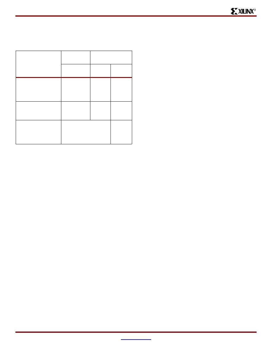
Table 7: Supported Destinations for Spartan/XL
Outputs
Destination
Spartan-XL
Outputs
Spartan
Outputs
3.3V, CMOS
5V,
TTL
5V,
CMOS
Any device,
VCC = 3.3V,
CMOS-threshold
inputs
√√
Some(1)
Any device,
VCC = 5V,
TTL-threshold inputs
√√
√
Any device,
VCC = 5V,
CMOS-threshold
inputs
Unreliable
Data
√
Notes:
1.
Only if destination device has 5V tolerant inputs.
相关PDF资料 |
PDF描述 |
|---|---|
| XCS10-5VQ240I | Spartan and Spartan-XL Families Field Programmable Gate Arrays |
| XCS10-5VQ256C | Spartan and Spartan-XL Families Field Programmable Gate Arrays |
| XCS10-5VQ256I | Spartan and Spartan-XL Families Field Programmable Gate Arrays |
| XCS10-5VQ280C | Spartan and Spartan-XL Families Field Programmable Gate Arrays |
| XCS10-5VQ280I | Spartan and Spartan-XL Families Field Programmable Gate Arrays |
相关代理商/技术参数 |
参数描述 |
|---|---|
| XCS10-5VQ240I | 制造商:XILINX 制造商全称:XILINX 功能描述:Spartan and Spartan-XL Families Field Programmable Gate Arrays |
| XCS10-5VQ256C | 制造商:XILINX 制造商全称:XILINX 功能描述:Spartan and Spartan-XL Families Field Programmable Gate Arrays |
| XCS10-5VQ256I | 制造商:XILINX 制造商全称:XILINX 功能描述:Spartan and Spartan-XL Families Field Programmable Gate Arrays |
| XCS10-5VQ280C | 制造商:XILINX 制造商全称:XILINX 功能描述:Spartan and Spartan-XL Families Field Programmable Gate Arrays |
| XCS10-5VQ280I | 制造商:XILINX 制造商全称:XILINX 功能描述:Spartan and Spartan-XL Families Field Programmable Gate Arrays |
发布紧急采购,3分钟左右您将得到回复。