参数资料
| 型号: | XCS20XL-4CS144C |
| 厂商: | Xilinx Inc |
| 文件页数: | 46/83页 |
| 文件大小: | 0K |
| 描述: | IC FPGA 3.3V C-TEMP HP 144CSBGA |
| 标准包装: | 1 |
| 系列: | Spartan®-XL |
| LAB/CLB数: | 400 |
| 逻辑元件/单元数: | 950 |
| RAM 位总计: | 12800 |
| 输入/输出数: | 113 |
| 门数: | 20000 |
| 电源电压: | 3 V ~ 3.6 V |
| 安装类型: | 表面贴装 |
| 工作温度: | 0°C ~ 85°C |
| 封装/外壳: | 144-TFBGA,CSPBGA |
| 供应商设备封装: | 144-LCSBGA(12x12) |
第1页第2页第3页第4页第5页第6页第7页第8页第9页第10页第11页第12页第13页第14页第15页第16页第17页第18页第19页第20页第21页第22页第23页第24页第25页第26页第27页第28页第29页第30页第31页第32页第33页第34页第35页第36页第37页第38页第39页第40页第41页第42页第43页第44页第45页当前第46页第47页第48页第49页第50页第51页第52页第53页第54页第55页第56页第57页第58页第59页第60页第61页第62页第63页第64页第65页第66页第67页第68页第69页第70页第71页第72页第73页第74页第75页第76页第77页第78页第79页第80页第81页第82页第83页
Spartan and Spartan-XL FPGA Families Data Sheet
50
DS060 (v2.0) March 1, 2013
Product Specification
R
Product Obsolete/Under Obsolescence
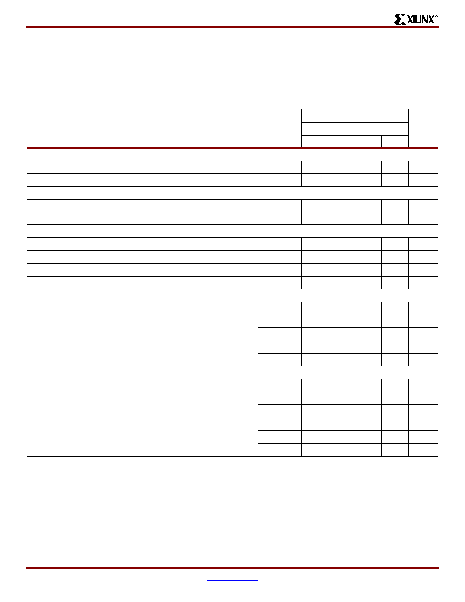
Spartan Family IOB Input Switching Characteristic Guidelines
All devices are 100% functionally tested. Internal timing
parameters are derived from measuring internal test pat-
terns. Listed below are representative values. For more
specific, more precise, and worst-case guaranteed data,
use the values reported by the static timing analyzer (TRCE
in the Xilinx Development System) and back-annotated to
the simulation netlist. These path delays, provided as a
guideline, have been extracted from the static timing ana-
lyzer report. All timing parameters assume worst-case oper-
ating conditions (supply voltage and junction temperature).
Symbol
Description
Device
Speed Grade
Units
-4
-3
Min
Max
Min
Max
Setup Times - TTL Inputs(1)
TECIK
Clock Enable (EC) to Clock (IK), no delay
All devices
1.6
-
2.1
-
ns
TPICK
Pad to Clock (IK), no delay
All devices
1.5
-
2.0
-
ns
Hold Times
TIKEC
Clock Enable (EC) to Clock (IK), no delay
All devices
0.0
-
0.9
-
ns
All Other Hold Times
All devices
0.0
-
0.0
-
ns
Propagation Delays - TTL Inputs(1)
TPID
Pad to I1, I2
All devices
-
1.5
-
2.0
ns
TPLI
Pad to I1, I2 via transparent input latch, no delay
All devices
-
2.8
-
3.6
ns
TIKRI
Clock (IK) to I1, I2 (flip-flop)
All devices
-
2.7
-
2.8
ns
TIKLI
Clock (IK) to I1, I2 (latch enable, active Low)
All devices
-
3.2
-
3.9
ns
Delay Adder for Input with Delay Option
TDelay
TECIKD = TECIK + TDelay
TPICKD = TPICK + TDelay
TPDLI = TPLI + TDelay
XCS05
3.6
-
4.0
-
ns
XCS10
3.7
-
4.1
-
ns
XCS20
3.8
-
4.2
-
ns
XCS30
4.5
-
5.0
-
ns
XCS40
5.5
-
5.5
-
ns
Global Set/Reset
TMRW
Minimum GSR pulse width
All devices
11.5
-
13.5
-
ns
TRRI
Delay from GSR input to any Q
XCS05
-
9.0
-
11.3
ns
XCS10
-
9.5
-
11.9
ns
XCS20
-
10.0
-
12.5
ns
XCS30
-
10.5
-
13.1
ns
XCS40
-
11.0
-
13.8
ns
Notes:
1.
Delay adder for CMOS Inputs option: for -3 speed grade, add 0.4 ns; for -4 speed grade, add 0.2 ns.
2.
Input pad setup and hold times are specified with respect to the internal clock (IK). For setup and hold times with respect to the clock
input, see the pin-to-pin parameters in the Pin-to-Pin Input Parameters table.
3.
Voltage levels of unused pads, bonded or unbonded, must be valid logic levels. Each can be configured with the internal pull-up
(default) or pull-down resistor, or configured as a driven output, or can be driven from an external source.
相关PDF资料 |
PDF描述 |
|---|---|
| XCS20-4VQ100C | IC FPGA 5V C-TEMP 100-VQFP |
| 65801-051LF | CLINCHER RECEPTACLE ASSY GOLD |
| 65801-155LF | CLINCHER RECEPTACLE ASSY GOLD |
| IDT7140SA35J8 | IC SRAM 8KBIT 35NS 52PLCC |
| IDT7130SA35J8 | IC SRAM 8KBIT 35NS 52PLCC |
相关代理商/技术参数 |
参数描述 |
|---|---|
| XCS20XL-4CS144I | 制造商:XILINX 制造商全称:XILINX 功能描述:Spartan and Spartan-XL Families Field Programmable Gate Arrays |
| XCS20XL-4CS208C | 制造商:XILINX 制造商全称:XILINX 功能描述:Spartan and Spartan-XL Families Field Programmable Gate Arrays |
| XCS20XL-4CS208I | 制造商:XILINX 制造商全称:XILINX 功能描述:Spartan and Spartan-XL Families Field Programmable Gate Arrays |
| XCS20XL-4CS240C | 制造商:XILINX 制造商全称:XILINX 功能描述:Spartan and Spartan-XL Families Field Programmable Gate Arrays |
| XCS20XL-4CS240I | 制造商:XILINX 制造商全称:XILINX 功能描述:Spartan and Spartan-XL Families Field Programmable Gate Arrays |
发布紧急采购,3分钟左右您将得到回复。