参数资料
| 型号: | XCS30XL-4TQ144C |
| 厂商: | Xilinx Inc |
| 文件页数: | 6/83页 |
| 文件大小: | 0K |
| 描述: | IC FPGA 3.3V C-TEMP HP 144TQFP |
| 产品变化通告: | Product Discontinuation 26/Oct/2011 |
| 标准包装: | 60 |
| 系列: | Spartan®-XL |
| LAB/CLB数: | 576 |
| 逻辑元件/单元数: | 1368 |
| RAM 位总计: | 18432 |
| 输入/输出数: | 113 |
| 门数: | 30000 |
| 电源电压: | 3 V ~ 3.6 V |
| 安装类型: | 表面贴装 |
| 工作温度: | 0°C ~ 85°C |
| 封装/外壳: | 144-LQFP |
| 供应商设备封装: | 144-TQFP(20x20) |
第1页第2页第3页第4页第5页当前第6页第7页第8页第9页第10页第11页第12页第13页第14页第15页第16页第17页第18页第19页第20页第21页第22页第23页第24页第25页第26页第27页第28页第29页第30页第31页第32页第33页第34页第35页第36页第37页第38页第39页第40页第41页第42页第43页第44页第45页第46页第47页第48页第49页第50页第51页第52页第53页第54页第55页第56页第57页第58页第59页第60页第61页第62页第63页第64页第65页第66页第67页第68页第69页第70页第71页第72页第73页第74页第75页第76页第77页第78页第79页第80页第81页第82页第83页
Spartan and Spartan-XL FPGA Families Data Sheet
14
DS060 (v2.0) March 1, 2013
Product Specification
R
Product Obsolete/Under Obsolescence
The 16 x 1 single-port configuration contains a RAM
array with 16 locations, each one-bit wide. One 4-bit
address decoder determines the RAM location for write
and read operations. There is one input for writing data
and one output for reading data, all at the selected
address.
The (16 x 1) x 2 single-port configuration combines two
16 x 1 single-port configurations (each according to the
preceding description). There is one data input, one
data output and one address decoder for each array.
These arrays can be addressed independently.
The 32 x 1 single-port configuration contains a RAM
array with 32 locations, each one-bit wide. There is one
data input, one data output, and one 5-bit address
decoder.
The dual-port mode 16 x 1 configuration contains a
RAM array with 16 locations, each one-bit wide. There
are two 4-bit address decoders, one for each port. One
port consists of an input for writing and an output for
reading, all at a selected address. The other port
consists of one output for reading from an
independently selected address.
The appropriate choice of RAM configuration mode for a
given design should be based on timing and resource
requirements, desired functionality, and the simplicity of the
design process. Selection criteria include the following:
Whereas the 32 x 1 single-port, the (16 x 1) x 2 single-port,
and the 16 x 1 dual-port configurations each use one entire
CLB, the 16 x 1 single-port configuration uses only one half
of a CLB. Due to its simultaneous read/write capability, the
dual-port RAM can transfer twice as much data as the sin-
gle-port RAM, which permits only one data operation at any
given time.
CLB memory configuration options are selected by using
the appropriate library symbol in the design entry.
Single-Port Mode
There are three CLB memory configurations for the sin-
gle-port RAM: 16 x 1, (16 x 1) x 2, and 32 x 1, the functional
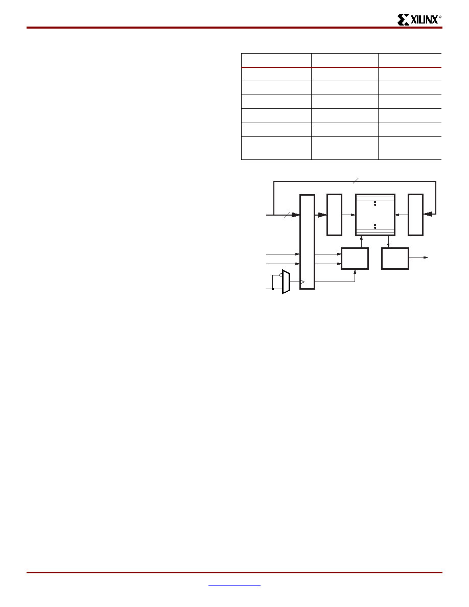
organization of which is shown in Figure 12.
The single-port RAM signals and the CLB signals (Figure 2,
page 4) from which they are originally derived are shown in
Writing data to the single-port RAM is essentially the same
as writing to a data register. It is an edge-triggered (syn-
chronous) operation performed by applying an address to
the A inputs and data to the D input during the active edge
of WCLK while WE is High.
The timing relationships are shown in Figure 13. The High
logic level on WE enables the input data register for writing.
The active edge of WCLK latches the address, input data,
and WE signals. Then, an internal write pulse is generated
that loads the data into the memory cell.
Table 9: Single-Port RAM Signals
RAM Signal
Function
CLB Signal
D0 or D1
Data In
DIN or H1
A[3:0]
Address
F[4:1] or G[4:1]
A4 (32 x 1 only)
Address
H1
WE
Write Enable
SR
WCLK
Clock
K
SPO
Single Port Out
(Data Out)
FOUT or GOUT
Notes:
1.
The (16 x 1) x 2 configuration combines two 16 x 1 single-port
RAMs, each with its own independent address bus and data
input. The same WE and WCLK signals are connected to both
RAMs.
2.
n = 4 for the 16 x 1 and (16 x 1) x 2 configurations. n = 5 for the
32 x 1 configuration.
Figure 12: Logic Diagram for the Single-Port RAM
WE
WCLK
A[n-1:0]
D0 or D1
n
SPO
INPUT
REGISTER
WRITE
R
O
W
SELECT
WRITE
CONTROL
READ
OUT
16 x 1
32 x 1
RAM ARRAY
READ
R
O
W
SELECT
DS060_12_043010
相关PDF资料 |
PDF描述 |
|---|---|
| ACB60DHAR-S793 | CONN EDGECARD 120PS .050 3.3V |
| HSC65DRYI-S734 | CONN EDGECARD 130PS DIP .100 SLD |
| FMC28DRYI | CONN EDGECARD 56POS DIP .100 SLD |
| AMM36DRYI | CONN EDGECARD 72POS DIP .156 SLD |
| RMC20DTES | CONN EDGECARD 40POS .100 EYELET |
相关代理商/技术参数 |
参数描述 |
|---|---|
| XCS30XL-4TQ144C0655 | 制造商:Xilinx 功能描述: |
| XCS30XL-4TQ144I | 功能描述:IC FPGA 3.3V I-TEMP HP 144TQFP RoHS:否 类别:集成电路 (IC) >> 嵌入式 - FPGA(现场可编程门阵列) 系列:Spartan®-XL 标准包装:1 系列:Kintex-7 LAB/CLB数:25475 逻辑元件/单元数:326080 RAM 位总计:16404480 输入/输出数:350 门数:- 电源电压:0.97 V ~ 1.03 V 安装类型:表面贴装 工作温度:0°C ~ 85°C 封装/外壳:900-BBGA,FCBGA 供应商设备封装:900-FCBGA(31x31) 其它名称:122-1789 |
| XCS30XL-4TQ208C | 制造商:XILINX 制造商全称:XILINX 功能描述:Spartan and Spartan-XL Families Field Programmable Gate Arrays |
| XCS30XL-4TQ208I | 制造商:XILINX 制造商全称:XILINX 功能描述:Spartan and Spartan-XL Families Field Programmable Gate Arrays |
| XCS30XL-4TQ240C | 制造商:XILINX 制造商全称:XILINX 功能描述:Spartan and Spartan-XL Families Field Programmable Gate Arrays |
发布紧急采购,3分钟左右您将得到回复。