参数资料
| 型号: | XCS30XL-4TQG144I |
| 厂商: | Xilinx Inc |
| 文件页数: | 8/83页 |
| 文件大小: | 0K |
| 描述: | IC SPARTAN-XL FPGA 30K 144-TQFP |
| 产品变化通告: | Product Discontinuation 26/Oct/2011 |
| 标准包装: | 60 |
| 系列: | Spartan®-XL |
| LAB/CLB数: | 576 |
| 逻辑元件/单元数: | 1368 |
| RAM 位总计: | 18432 |
| 输入/输出数: | 113 |
| 门数: | 30000 |
| 电源电压: | 3 V ~ 3.6 V |
| 安装类型: | 表面贴装 |
| 工作温度: | -40°C ~ 100°C |
| 封装/外壳: | 144-LQFP |
| 供应商设备封装: | 144-TQFP(20x20) |
| 其它名称: | 122-1298 |
第1页第2页第3页第4页第5页第6页第7页当前第8页第9页第10页第11页第12页第13页第14页第15页第16页第17页第18页第19页第20页第21页第22页第23页第24页第25页第26页第27页第28页第29页第30页第31页第32页第33页第34页第35页第36页第37页第38页第39页第40页第41页第42页第43页第44页第45页第46页第47页第48页第49页第50页第51页第52页第53页第54页第55页第56页第57页第58页第59页第60页第61页第62页第63页第64页第65页第66页第67页第68页第69页第70页第71页第72页第73页第74页第75页第76页第77页第78页第79页第80页第81页第82页第83页
Spartan and Spartan-XL FPGA Families Data Sheet
16
DS060 (v2.0) March 1, 2013
Product Specification
R
Product Obsolete/Under Obsolescence
CLB signals from which they are originally derived are
shown in Table 10.
The RAM16X1D primitive used to instantiate the dual-port
RAM consists of an upper and a lower 16 x 1 memory array.
The address port labeled A[3:0] supplies both the read and
write addresses for the lower memory array, which behaves
the same as the 16 x 1 single-port RAM array described
previously. Single Port Out (SPO) serves as the data output
for the lower memory. Therefore, SPO reflects the data at
address A[3:0].
The other address port, labeled DPRA[3:0] for Dual Port
Read Address, supplies the read address for the upper
memory. The write address for this memory, however,
comes from the address A[3:0]. Dual Port Out (DPO) serves
as the data output for the upper memory. Therefore, DPO
reflects the data at address DPRA[3:0].
By using A[3:0] for the write address and DPRA[3:0] for the
read address, and reading only the DPO output, a FIFO that
can read and write simultaneously is easily generated. The
simultaneous
read/write
capability
possible
with
the
dual-port RAM can provide twice the effective data through-
put of a single-port RAM alternating read and write opera-
tions.
The timing relationships for the dual-port RAM mode are
shown in Figure 13.
Note that write operations to RAM are synchronous
(edge-triggered); however, data access is asynchronous.
Initializing RAM at FPGA Configuration
Both RAM and ROM implementations in the Spartan/XL
families are initialized during device configuration. The initial
contents are defined via an INIT attribute or property
attached to the RAM or ROM symbol, as described in the
library guide. If not defined, all RAM contents are initialized
to zeros, by default.
RAM initialization occurs only during device configuration.
The RAM content is not affected by GSR.
More Information on Using RAM Inside CLBs
Three application notes are available from Xilinx that dis-
cuss synchronous (edge-triggered) RAM: "Xilinx Edge-Trig-
gered and Dual-Port RAM Capability," "Implementing FIFOs
in Xilinx RAM," and "Synchronous and Asynchronous FIFO
Designs." All three application notes apply to both the Spar-
tan and the Spartan-XL families.
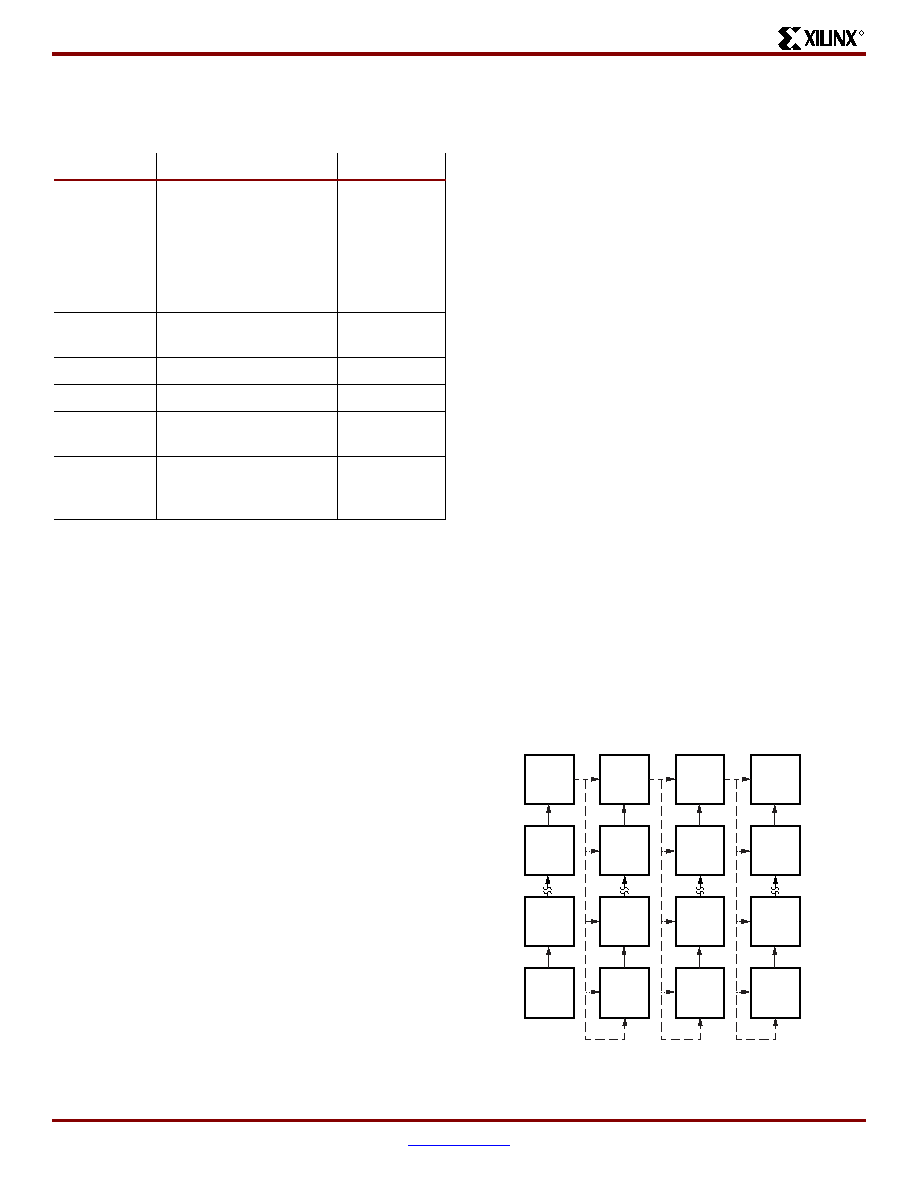
Fast Carry Logic
Each CLB F-LUT and G-LUT contains dedicated arithmetic
logic for the fast generation of carry and borrow signals.
This extra output is passed on to the function generator in
the adjacent CLB. The carry chain is independent of normal
routing resources. (See Figure 15.)
Dedicated fast carry logic greatly increases the efficiency
and performance of adders, subtractors, accumulators,
comparators and counters. It also opens the door to many
new applications involving arithmetic operation, where the
previous generations of FPGAs were not fast enough or too
inefficient. High-speed address offset calculations in micro-
processor or graphics systems, and high-speed addition in
digital signal processing are two typical applications.
The two 4-input function generators can be configured as a
2-bit adder with built-in hidden carry that can be expanded
to any length. This dedicated carry circuitry is so fast and
efficient that conventional speed-up methods like carry gen-
erate/propagate are meaningless even at the 16-bit level,
and of marginal benefit at the 32-bit level. This fast carry
logic is one of the more significant features of the Spartan
Table 10: Dual-Port RAM Signals
RAM Signal
Function
CLB Signal
D
Data In
DIN
A[3:0]
Read Address for
Single-Port.
Write Address for
Single-Port and
Dual-Port.
F[4:1]
DPRA[3:0]
Read Address for
Dual-Port
G[4:1]
WE
Write Enable
SR
WCLK
Clock
K
SPO
Single Port Out
(addressed by A[3:0])
FOUT
DPO
Dual Port Out
(addressed by
DPRA[3:0])
GOUT
Figure 15: Available Spartan/XL Carry Propagation
Paths
CLB
DS060_15_081100
相关PDF资料 |
PDF描述 |
|---|---|
| XC5VLX30-1FFG324CES | IC FPGA VIRTEX-5 ES 30K 324-FBGA |
| IDT71V65903S85PFG8 | IC SRAM 9MBIT 85NS 100TQFP |
| IDT71V65903S80PFG8 | IC SRAM 9MBIT 80NS 100TQFP |
| IDT71V65803S133PFG8 | IC SRAM 9MBIT 133MHZ 100TQFP |
| IDT71V65803S100PFG8 | IC SRAM 9MBIT 100MHZ 100TQFP |
相关代理商/技术参数 |
参数描述 |
|---|---|
| XCS30XL-4VQ100C | 功能描述:IC FPGA 3.3V C-TEMP HP 100VQFP RoHS:否 类别:集成电路 (IC) >> 嵌入式 - FPGA(现场可编程门阵列) 系列:Spartan®-XL 标准包装:1 系列:Kintex-7 LAB/CLB数:25475 逻辑元件/单元数:326080 RAM 位总计:16404480 输入/输出数:350 门数:- 电源电压:0.97 V ~ 1.03 V 安装类型:表面贴装 工作温度:0°C ~ 85°C 封装/外壳:900-BBGA,FCBGA 供应商设备封装:900-FCBGA(31x31) 其它名称:122-1789 |
| XCS30XL-4VQ100I | 功能描述:IC FPGA 3.3V I-TEMP HP 100VQFP RoHS:否 类别:集成电路 (IC) >> 嵌入式 - FPGA(现场可编程门阵列) 系列:Spartan®-XL 标准包装:1 系列:Kintex-7 LAB/CLB数:25475 逻辑元件/单元数:326080 RAM 位总计:16404480 输入/输出数:350 门数:- 电源电压:0.97 V ~ 1.03 V 安装类型:表面贴装 工作温度:0°C ~ 85°C 封装/外壳:900-BBGA,FCBGA 供应商设备封装:900-FCBGA(31x31) 其它名称:122-1789 |
| XCS30XL-4VQ144C | 制造商:XILINX 制造商全称:XILINX 功能描述:Spartan and Spartan-XL Families Field Programmable Gate Arrays |
| XCS30XL-4VQ144I | 制造商:XILINX 制造商全称:XILINX 功能描述:Spartan and Spartan-XL Families Field Programmable Gate Arrays |
| XCS30XL-4VQ208C | 制造商:XILINX 制造商全称:XILINX 功能描述:Spartan and Spartan-XL Families Field Programmable Gate Arrays |
发布紧急采购,3分钟左右您将得到回复。