参数资料
| 型号: | XCV200E-7FG256I |
| 厂商: | Xilinx Inc |
| 文件页数: | 159/233页 |
| 文件大小: | 0K |
| 描述: | IC FPGA 1.8V I-TEMP 256-FBGA |
| 产品变化通告: | FPGA Family Discontinuation 18/Apr/2011 |
| 标准包装: | 90 |
| 系列: | Virtex®-E |
| LAB/CLB数: | 1176 |
| 逻辑元件/单元数: | 5292 |
| RAM 位总计: | 114688 |
| 输入/输出数: | 176 |
| 门数: | 306393 |
| 电源电压: | 1.71 V ~ 1.89 V |
| 安装类型: | 表面贴装 |
| 工作温度: | -40°C ~ 100°C |
| 封装/外壳: | 256-BGA |
| 供应商设备封装: | 256-FBGA(17x17) |
第1页第2页第3页第4页第5页第6页第7页第8页第9页第10页第11页第12页第13页第14页第15页第16页第17页第18页第19页第20页第21页第22页第23页第24页第25页第26页第27页第28页第29页第30页第31页第32页第33页第34页第35页第36页第37页第38页第39页第40页第41页第42页第43页第44页第45页第46页第47页第48页第49页第50页第51页第52页第53页第54页第55页第56页第57页第58页第59页第60页第61页第62页第63页第64页第65页第66页第67页第68页第69页第70页第71页第72页第73页第74页第75页第76页第77页第78页第79页第80页第81页第82页第83页第84页第85页第86页第87页第88页第89页第90页第91页第92页第93页第94页第95页第96页第97页第98页第99页第100页第101页第102页第103页第104页第105页第106页第107页第108页第109页第110页第111页第112页第113页第114页第115页第116页第117页第118页第119页第120页第121页第122页第123页第124页第125页第126页第127页第128页第129页第130页第131页第132页第133页第134页第135页第136页第137页第138页第139页第140页第141页第142页第143页第144页第145页第146页第147页第148页第149页第150页第151页第152页第153页第154页第155页第156页第157页第158页当前第159页第160页第161页第162页第163页第164页第165页第166页第167页第168页第169页第170页第171页第172页第173页第174页第175页第176页第177页第178页第179页第180页第181页第182页第183页第184页第185页第186页第187页第188页第189页第190页第191页第192页第193页第194页第195页第196页第197页第198页第199页第200页第201页第202页第203页第204页第205页第206页第207页第208页第209页第210页第211页第212页第213页第214页第215页第216页第217页第218页第219页第220页第221页第222页第223页第224页第225页第226页第227页第228页第229页第230页第231页第232页第233页
Virtex-E 1.8 V Field Programmable Gate Arrays
R
DS022-2 (v3.0) March 21, 2014
Module 2 of 4
Production Product Specification
25
— OBSOLETE — OBSOLETE — OBSOLETE — OBSOLETE —
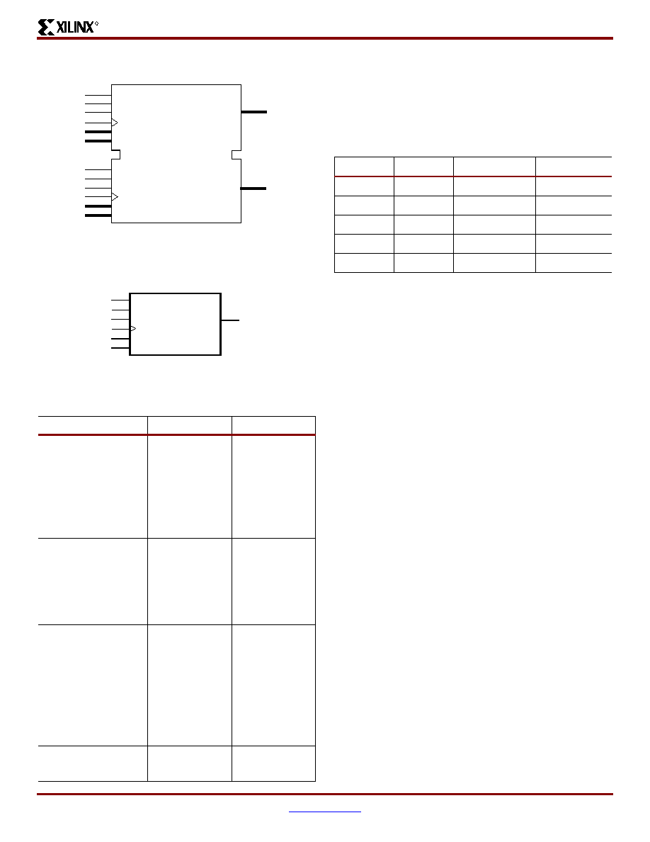
Port Signals
Each block SelectRAM+ port operates independently of the
others while accessing the same set of 4096 memory cells.
Table 15 describes the depth and width aspect ratios for the
block SelectRAM+ memory.
Clock—CLK[A|B]
Each port is fully synchronous with independent clock pins.
All port input pins have setup time referenced to the port
CLK pin. The data output bus has a clock-to-out time refer-
enced to the CLK pin.
Enable—EN[A|B]
The enable pin affects the read, write and reset functionality
of the port. Ports with an inactive enable pin keep the output
pins in the previous state and do not write data to the mem-
ory cells.
Write Enable—WE[A|B]
Activating the write enable pin allows the port to write to the
memory cells. When active, the contents of the data input
bus are written to the RAM at the address pointed to by the
address bus, and the new data also reflects on the data out
bus. When inactive, a read operation occurs and the con-
tents of the memory cells referenced by the address bus
reflect on the data out bus.
Reset—RST[A|B]
The reset pin forces the data output bus latches to zero syn-
chronously. This does not affect the memory cells of the
RAM and does not disturb a write operation on the other
port.
Address Bus—ADDR[A|B]<#:0>
The address bus selects the memory cells for read or write.
The width of the port determines the required width of this
bus as shown in Table 15.
Data In Bus—DI[A|B]<#:0>
The data in bus provides the new data value to be written
into the RAM. This bus and the port have the same width, as
shown in Table 15.
Figure 31: Dual-Port Block SelectRAM+ Memory
Figure 32: Single-Port Block SelectRAM+ Memory
Table 14: Available Library Primitives
Primitive
Port A Width
Port B Width
RAMB4_S1
RAMB4_S1_S1
RAMB4_S1_S2
RAMB4_S1_S4
RAMB4_S1_S8
RAMB4_S1_S16
1
N/A
1
2
4
8
16
RAMB4_S2
RAMB4_S2_S2
RAMB4_S2_S4
RAMB4_S2_S8
RAMB4_S2_S16
2
N/A
2
4
8
16
RAMB4_S4
RAMB4_S4_S4
RAMB4_S4_S8
RAMB4_S4_S16
4
N/A
4
8
16
RAMB4_S8
RAMB4_S8_S8
RAMB4_S8_S16
8
N/A
8
16
RAMB4_S16
RAMB4_S16_S16
16
N/A
16
WEB
ENB
RSTB
CLKB
ADDRB[#:0]
DIB[#:0]
WEA
ENA
RSTA
CLKA
ADDRA[#:0]
DIA[#:0]
DOA[#:0]
DOB[#:0]
RAMB4_S#_S#
ds022_032_121399
ds022_033_121399
DO[#:0]
WE
EN
RST
CLK
ADDR[#:0]
DI[#:0]
RAMB4_S#
Table 15: Block SelectRAM+ Port Aspect Ratios
Width
Depth
ADDR Bus
Data Bus
1
4096
ADDR<11:0>
DATA<0>
2
2048
ADDR<10:0>
DATA<1:0>
4
1024
ADDR<9:0>
DATA<3:0>
8
512
ADDR<8:0>
DATA<7:0>
16
256
ADDR<7:0>
DATA<15:0>
相关PDF资料 |
PDF描述 |
|---|---|
| SST39SF020A-45-4C-WHE | IC FLASH MPF 2MBIT 45NS 32TSOP |
| SST39SF020A-70-4I-WHE | IC FLASH MPF 2MBIT 70NS 32TSOP |
| XC6SLX150T-3FGG900C | IC FPGA SPARTAN 6 147K 900FGGBGA |
| SST39SF020A-55-4C-NHE-T | IC FLASH MPF 2MBIT 55NS 32PLCC |
| SST39SF020A-55-4I-NHE-T | IC FLASH MPF 2MB 55NS 32PLCC |
相关代理商/技术参数 |
参数描述 |
|---|---|
| XCV200E-7FG456C | 功能描述:IC FPGA 1.8V C-TEMP 456-FBGA RoHS:否 类别:集成电路 (IC) >> 嵌入式 - FPGA(现场可编程门阵列) 系列:Virtex®-E 产品变化通告:Step Intro and Pkg Change 11/March/2008 标准包装:1 系列:Virtex®-5 SXT LAB/CLB数:4080 逻辑元件/单元数:52224 RAM 位总计:4866048 输入/输出数:480 门数:- 电源电压:0.95 V ~ 1.05 V 安装类型:表面贴装 工作温度:-40°C ~ 100°C 封装/外壳:1136-BBGA,FCBGA 供应商设备封装:1136-FCBGA 配用:568-5088-ND - BOARD DEMO DAC1408D750122-1796-ND - EVALUATION PLATFORM VIRTEX-5 |
| XCV200E-7FG456I | 功能描述:IC FPGA 1.8V I-TEMP 456-FBGA RoHS:否 类别:集成电路 (IC) >> 嵌入式 - FPGA(现场可编程门阵列) 系列:Virtex®-E 产品变化通告:Step Intro and Pkg Change 11/March/2008 标准包装:1 系列:Virtex®-5 SXT LAB/CLB数:4080 逻辑元件/单元数:52224 RAM 位总计:4866048 输入/输出数:480 门数:- 电源电压:0.95 V ~ 1.05 V 安装类型:表面贴装 工作温度:-40°C ~ 100°C 封装/外壳:1136-BBGA,FCBGA 供应商设备封装:1136-FCBGA 配用:568-5088-ND - BOARD DEMO DAC1408D750122-1796-ND - EVALUATION PLATFORM VIRTEX-5 |
| XCV200E-7HQ240C | 制造商:XILINX 制造商全称:XILINX 功能描述:Virtex-E 1.8 V Field Programmable Gate Arrays |
| XCV200E-7HQ240I | 制造商:XILINX 制造商全称:XILINX 功能描述:Virtex⑩-E 1.8 V Field Programmable Gate Arrays |
| XCV200E-7PQ240C | 功能描述:IC FPGA 1.8V C-TEMP 240-PQFP RoHS:否 类别:集成电路 (IC) >> 嵌入式 - FPGA(现场可编程门阵列) 系列:Virtex®-E 产品变化通告:Step Intro and Pkg Change 11/March/2008 标准包装:1 系列:Virtex®-5 SXT LAB/CLB数:4080 逻辑元件/单元数:52224 RAM 位总计:4866048 输入/输出数:480 门数:- 电源电压:0.95 V ~ 1.05 V 安装类型:表面贴装 工作温度:-40°C ~ 100°C 封装/外壳:1136-BBGA,FCBGA 供应商设备封装:1136-FCBGA 配用:568-5088-ND - BOARD DEMO DAC1408D750122-1796-ND - EVALUATION PLATFORM VIRTEX-5 |
发布紧急采购,3分钟左右您将得到回复。