参数资料
| 型号: | XCV200E-8PQ240C |
| 厂商: | Xilinx Inc |
| 文件页数: | 13/233页 |
| 文件大小: | 0K |
| 描述: | IC FPGA 1.8V C-TEMP 240-PQFP |
| 产品变化通告: | FPGA Family Discontinuation 18/Apr/2011 |
| 标准包装: | 24 |
| 系列: | Virtex®-E |
| LAB/CLB数: | 1176 |
| 逻辑元件/单元数: | 5292 |
| RAM 位总计: | 114688 |
| 输入/输出数: | 158 |
| 门数: | 306393 |
| 电源电压: | 1.71 V ~ 1.89 V |
| 安装类型: | 表面贴装 |
| 工作温度: | 0°C ~ 85°C |
| 封装/外壳: | 240-BFQFP |
| 供应商设备封装: | 240-PQFP(32x32) |
第1页第2页第3页第4页第5页第6页第7页第8页第9页第10页第11页第12页当前第13页第14页第15页第16页第17页第18页第19页第20页第21页第22页第23页第24页第25页第26页第27页第28页第29页第30页第31页第32页第33页第34页第35页第36页第37页第38页第39页第40页第41页第42页第43页第44页第45页第46页第47页第48页第49页第50页第51页第52页第53页第54页第55页第56页第57页第58页第59页第60页第61页第62页第63页第64页第65页第66页第67页第68页第69页第70页第71页第72页第73页第74页第75页第76页第77页第78页第79页第80页第81页第82页第83页第84页第85页第86页第87页第88页第89页第90页第91页第92页第93页第94页第95页第96页第97页第98页第99页第100页第101页第102页第103页第104页第105页第106页第107页第108页第109页第110页第111页第112页第113页第114页第115页第116页第117页第118页第119页第120页第121页第122页第123页第124页第125页第126页第127页第128页第129页第130页第131页第132页第133页第134页第135页第136页第137页第138页第139页第140页第141页第142页第143页第144页第145页第146页第147页第148页第149页第150页第151页第152页第153页第154页第155页第156页第157页第158页第159页第160页第161页第162页第163页第164页第165页第166页第167页第168页第169页第170页第171页第172页第173页第174页第175页第176页第177页第178页第179页第180页第181页第182页第183页第184页第185页第186页第187页第188页第189页第190页第191页第192页第193页第194页第195页第196页第197页第198页第199页第200页第201页第202页第203页第204页第205页第206页第207页第208页第209页第210页第211页第212页第213页第214页第215页第216页第217页第218页第219页第220页第221页第222页第223页第224页第225页第226页第227页第228页第229页第230页第231页第232页第233页
Virtex-E 1.8 V Field Programmable Gate Arrays
R
DS022-2 (v3.0) March 21, 2014
Module 2 of 4
Production Product Specification
5
— OBSOLETE — OBSOLETE — OBSOLETE — OBSOLETE —
forces a storage element into the initialization state speci-
fied for it in the configuration. BY forces it into the opposite
state. Alternatively, these signals can be configured to oper-
ate asynchronously. All of the control signals are indepen-
dently invertible, and are shared by the two flip-flops within
the slice.
Additional Logic
The F5 multiplexer in each slice combines the function gen-
erator outputs. This combination provides either a function
generator that can implement any 5-input function, a 4:1
multiplexer, or selected functions of up to nine inputs.
Similarly, the F6 multiplexer combines the outputs of all four
function generators in the CLB by selecting one of the
F5-multiplexer outputs. This permits the implementation of
any 6-input function, an 8:1 multiplexer, or selected func-
tions of up to 19 inputs.
Each CLB has four direct feedthrough paths, two per slice.
These paths provide extra data input lines or additional local
routing that does not consume logic resources.
Arithmetic Logic
Dedicated carry logic provides fast arithmetic carry capabil-
ity for high-speed arithmetic functions. The Virtex-E CLB
supports two separate carry chains, one per Slice. The
height of the carry chains is two bits per CLB.
The arithmetic logic includes an XOR gate that allows a
2-bit full adder to be implemented within a slice. In addition,
a dedicated AND gate improves the efficiency of multiplier
implementation. The dedicated carry path can also be used
to cascade function generators for implementing wide logic
functions.
BUFTs
Each Virtex-E CLB contains two 3-state drivers (BUFTs)
that can drive on-chip buses. See Dedicated Routing.
Each Virtex-E BUFT has an independent 3-state control pin
and an independent input pin.
Block SelectRAM
Virtex-E FPGAs incorporate large block SelectRAM memo-
ries. These complement the Distributed SelectRAM memo-
ries that provide shallow RAM structures implemented in
CLBs.
Block SelectRAM memory blocks are organized in columns,
starting at the left (column 0) and right outside edges and
inserted every 12 CLB columns (see notes for smaller
devices). Each memory block is four CLBs high, and each
memory column extends the full height of the chip, immedi-
ately adjacent (to the right, except for column 0) of the CLB
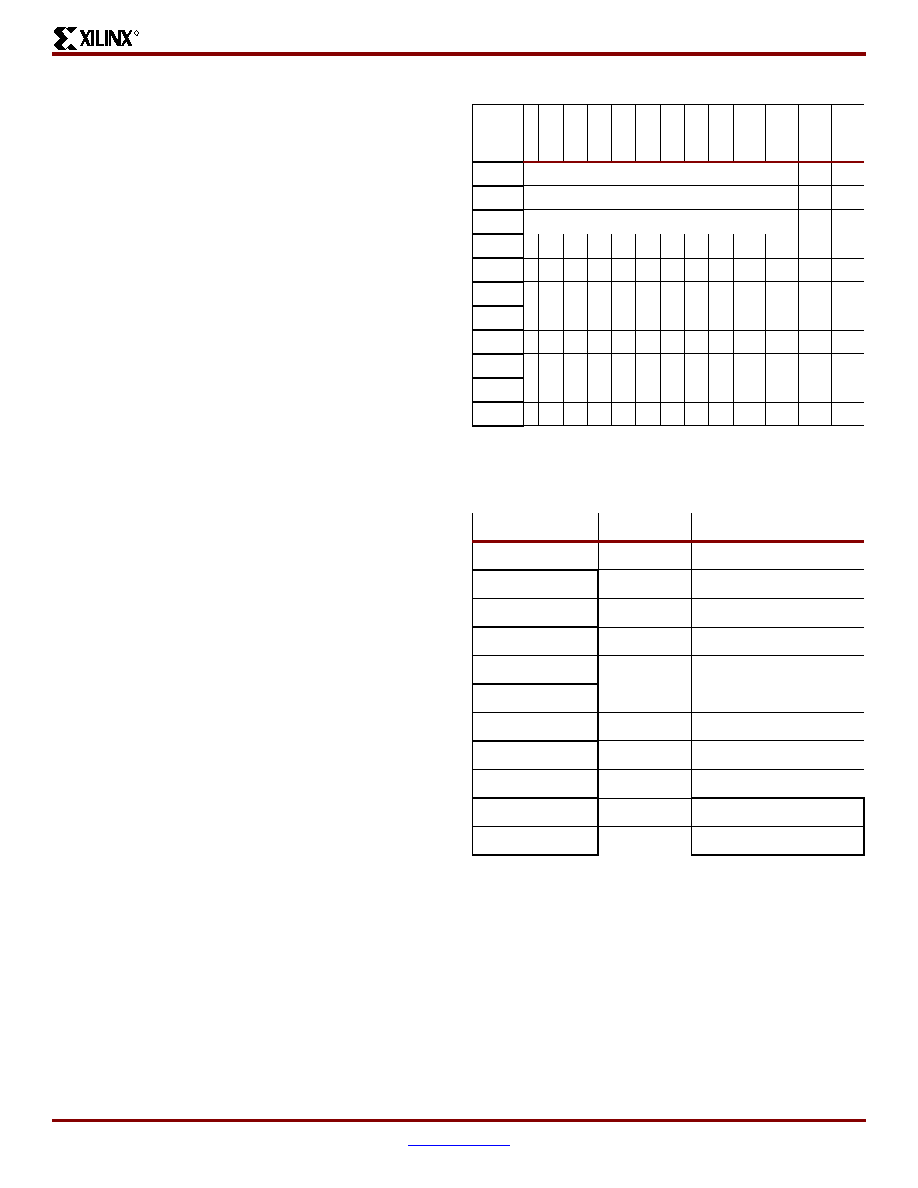
column locations indicated in Table 3.
Table 4 shows the amount of block SelectRAM memory that
is available in each Virtex-E device.
As illustrated in Figure 6, each block SelectRAM cell is a
fully synchronous dual-ported (True Dual Port) 4096-bit
RAM with independent control signals for each port. The
data widths of the two ports can be configured indepen-
dently, providing built-in bus-width conversion.
Table 3: CLB/Block RAM Column Locations
XCV
Device
/Col.
0 12 24364860728496
108
120
138
156
50E
Columns 0, 6, 18, & 24
100E
Columns 0, 12, 18, & 30
200E
Columns 0, 12, 30, & 42
300E
√√
√
400E
√√
√
600E
√√
√
1000E
√ √
√
√√√
1600E
√ √√√
√√√
√
2000E
√ √√√
√√
√
2600E
√ √√√
√
3200E
√ √
√
√√√√
Table 4: Virtex-E Block SelectRAM Amounts
Virtex-E Device
# of Blocks
Block SelectRAM Bits
XCV50E
16
65,536
XCV100E
20
81,920
XCV200E
28
114,688
XCV300E
32
131,072
XCV400E
40
163,840
XCV600E
72
294,912
XCV1000E
96
393,216
XCV1600E
144
589,824
XCV2000E
160
655,360
XCV2600E
184
753,664
XCV3200E
208
851,968
相关PDF资料 |
PDF描述 |
|---|---|
| SST39WF400B-70-4I-MAQE | IC FLASH MPF 4MBIT 70NS 48WFBGA |
| XC2V1000-4FGG256I | IC FPGA VIRTEX-II 2M 256-FBGA |
| SST39WF400B-70-4C-MAQE-T | IC FLASH MPF 4MBIT 70NS 48WFBGA |
| SST39WF400B-70-4I-B3KE-T | IC FLASH MPF 4MBIT 70NS 48TFBGA |
| XC2V1000-5FGG256C | IC VIRTEX-II FPGA 1M 256-FBGA |
相关代理商/技术参数 |
参数描述 |
|---|---|
| XCV200E-8PQ240I | 制造商:XILINX 制造商全称:XILINX 功能描述:Virtex-E 1.8 V Field Programmable Gate Arrays |
| XCV200FG-456AFP | 制造商:Xilinx 功能描述: |
| XCV2600E | 制造商:XILINX 制造商全称:XILINX 功能描述:Field Programmable Gate Arrays |
| XCV2600E-6BG240C | 制造商:XILINX 制造商全称:XILINX 功能描述:Virtex-E 1.8 V Field Programmable Gate Arrays |
| XCV2600E-6BG240I | 制造商:XILINX 制造商全称:XILINX 功能描述:Virtex⑩-E 1.8 V Field Programmable Gate Arrays |
发布紧急采购,3分钟左右您将得到回复。