参数资料
| 型号: | XCV300E-6PQ240I |
| 厂商: | Xilinx Inc |
| 文件页数: | 57/233页 |
| 文件大小: | 0K |
| 描述: | IC FPGA 1.8V I-TEMP 240-PQFP |
| 产品变化通告: | FPGA Family Discontinuation 18/Apr/2011 |
| 标准包装: | 24 |
| 系列: | Virtex®-E |
| LAB/CLB数: | 1536 |
| 逻辑元件/单元数: | 6912 |
| RAM 位总计: | 131072 |
| 输入/输出数: | 158 |
| 门数: | 411955 |
| 电源电压: | 1.71 V ~ 1.89 V |
| 安装类型: | 表面贴装 |
| 工作温度: | -40°C ~ 100°C |
| 封装/外壳: | 240-BFQFP |
| 供应商设备封装: | 240-PQFP(32x32) |
第1页第2页第3页第4页第5页第6页第7页第8页第9页第10页第11页第12页第13页第14页第15页第16页第17页第18页第19页第20页第21页第22页第23页第24页第25页第26页第27页第28页第29页第30页第31页第32页第33页第34页第35页第36页第37页第38页第39页第40页第41页第42页第43页第44页第45页第46页第47页第48页第49页第50页第51页第52页第53页第54页第55页第56页当前第57页第58页第59页第60页第61页第62页第63页第64页第65页第66页第67页第68页第69页第70页第71页第72页第73页第74页第75页第76页第77页第78页第79页第80页第81页第82页第83页第84页第85页第86页第87页第88页第89页第90页第91页第92页第93页第94页第95页第96页第97页第98页第99页第100页第101页第102页第103页第104页第105页第106页第107页第108页第109页第110页第111页第112页第113页第114页第115页第116页第117页第118页第119页第120页第121页第122页第123页第124页第125页第126页第127页第128页第129页第130页第131页第132页第133页第134页第135页第136页第137页第138页第139页第140页第141页第142页第143页第144页第145页第146页第147页第148页第149页第150页第151页第152页第153页第154页第155页第156页第157页第158页第159页第160页第161页第162页第163页第164页第165页第166页第167页第168页第169页第170页第171页第172页第173页第174页第175页第176页第177页第178页第179页第180页第181页第182页第183页第184页第185页第186页第187页第188页第189页第190页第191页第192页第193页第194页第195页第196页第197页第198页第199页第200页第201页第202页第203页第204页第205页第206页第207页第208页第209页第210页第211页第212页第213页第214页第215页第216页第217页第218页第219页第220页第221页第222页第223页第224页第225页第226页第227页第228页第229页第230页第231页第232页第233页
Virtex-E 1.8 V Field Programmable Gate Arrays
R
DS022-2 (v3.0) March 21, 2014
Module 2 of 4
Production Product Specification
9
— OBSOLETE — OBSOLETE — OBSOLETE — OBSOLETE —
Instruction Set
The Virtex-E series Boundary Scan instruction set also
includes instructions to configure the device and read back
configuration data (CFG_IN, CFG_OUT, and JSTART). The
complete instruction set is coded as shown in Table 6..
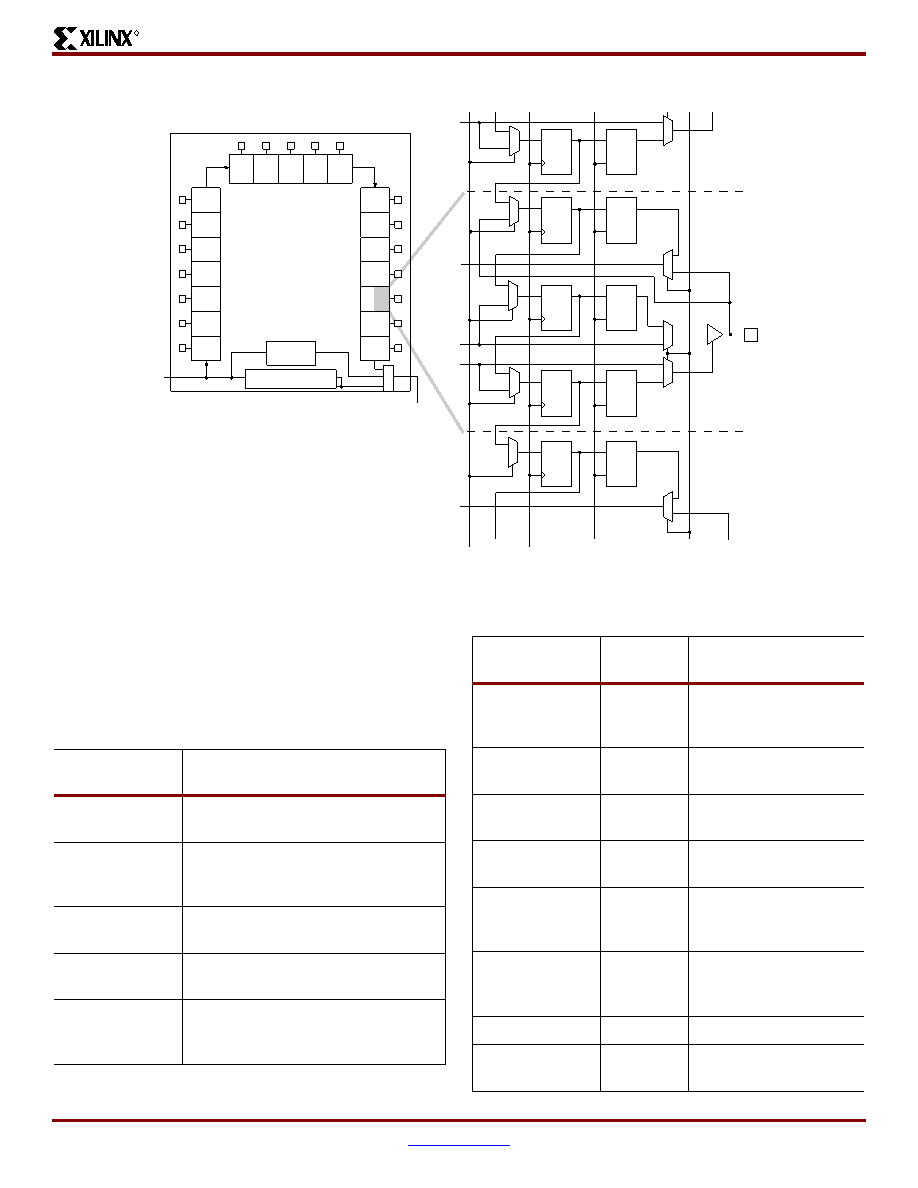
Figure 11: Virtex-E Family Boundary Scan Logic
D
Q
D
Q
IOB
M
U
X
BYPASS
REGISTER
IOB
TDO
TDI
IOB
1
0
1
0
1
0
1
0
1
0
sd
LE
DQ
D
Q
D
Q
1
0
1
0
1
0
1
0
DQ
LE
sd
LE
DQ
sd
LE
DQ
IOB
D
Q
1
0
DQ
LE
sd
IOB.T
DATA IN
IOB.I
IOB.Q
IOB.T
IOB.I
SHIFT/
CAPTURE
CLOCK DATA
REGISTER
DATAOUT
UPDATE
EXTEST
X9016
INSTRUCTION REGISTER
Table 6: Boundary Scan Instructions
Boundary Scan
Command
Binary
Code(4:0)
Description
EXTEST
00000
Enables Boundary Scan
EXTEST operation
SAMPLE/
PRELOAD
00001
Enables Boundary Scan
SAMPLE/PRELOAD
operation
USER1
00010
Access user-defined
register 1
USER2
00011
Access user-defined
register 2
CFG_OUT
00100
Access the
configuration bus for
read operations.
CFG_IN
00101
Access the
configuration bus for
write operations.
INTEST
00111
Enables Boundary Scan
INTEST operation
USERCODE
01000
Enables shifting out
USER code
IDCODE
01001
Enables shifting out of
ID Code
HIGHZ
01010
3-states output pins
while enabling the
Bypass Register
JSTART
01100
Clock the start-up
sequence when
StartupClk is TCK
BYPASS
11111
Enables BYPASS
RESERVED
All other
codes
Xilinx reserved
instructions
Table 6: Boundary Scan Instructions (Continued)
Boundary Scan
Command
Binary
Code(4:0)
Description
相关PDF资料 |
PDF描述 |
|---|---|
| XCV300E-7FG256C | IC FPGA 1.8V C-TEMP 256-FBGA |
| SST39WF1602-70-4C-MAQE-T | IC MEM MPF 16MBIT FLASH 48WFBGA |
| SST39WF1602-70-4C-MAQE | IC FLASH MPF 16MBIT 70NS 48WFBGA |
| XC4VSX25-10FFG668I | IC FPGA VIRTEX-4 SX 25K 668FCBGA |
| SST39VF1602-70-4C-B3KE | IC FLASH MPF 16MBIT 70NS 48TFBGA |
相关代理商/技术参数 |
参数描述 |
|---|---|
| XCV300E-6TQ144C | 制造商:XILINX 制造商全称:XILINX 功能描述:Field Programmable Gate Arrays |
| XCV300E-6TQ144I | 制造商:XILINX 制造商全称:XILINX 功能描述:Field Programmable Gate Arrays |
| XCV300E-7BG204C | 制造商:XILINX 制造商全称:XILINX 功能描述:Virte -E 1.8 V Field Programmable Gate Arrays |
| XCV300E-7BG204I | 制造商:XILINX 制造商全称:XILINX 功能描述:Virte -E 1.8 V Field Programmable Gate Arrays |
| XCV300E-7BG240C | 制造商:XILINX 制造商全称:XILINX 功能描述:Virtex⑩-E 1.8 V Field Programmable Gate Arrays |
发布紧急采购,3分钟左右您将得到回复。