参数资料
| 型号: | XCV300E-8BG352C |
| 厂商: | Xilinx Inc |
| 文件页数: | 154/233页 |
| 文件大小: | 0K |
| 描述: | IC FPGA 1.8V C-TEMP 352-MBGA |
| 产品变化通告: | FPGA Family Discontinuation 18/Apr/2011 |
| 标准包装: | 1 |
| 系列: | Virtex®-E |
| LAB/CLB数: | 1536 |
| 逻辑元件/单元数: | 6912 |
| RAM 位总计: | 131072 |
| 输入/输出数: | 260 |
| 门数: | 411955 |
| 电源电压: | 1.71 V ~ 1.89 V |
| 安装类型: | 表面贴装 |
| 工作温度: | 0°C ~ 85°C |
| 封装/外壳: | 352-LBGA,金属 |
| 供应商设备封装: | 352-MBGA(35x35) |
第1页第2页第3页第4页第5页第6页第7页第8页第9页第10页第11页第12页第13页第14页第15页第16页第17页第18页第19页第20页第21页第22页第23页第24页第25页第26页第27页第28页第29页第30页第31页第32页第33页第34页第35页第36页第37页第38页第39页第40页第41页第42页第43页第44页第45页第46页第47页第48页第49页第50页第51页第52页第53页第54页第55页第56页第57页第58页第59页第60页第61页第62页第63页第64页第65页第66页第67页第68页第69页第70页第71页第72页第73页第74页第75页第76页第77页第78页第79页第80页第81页第82页第83页第84页第85页第86页第87页第88页第89页第90页第91页第92页第93页第94页第95页第96页第97页第98页第99页第100页第101页第102页第103页第104页第105页第106页第107页第108页第109页第110页第111页第112页第113页第114页第115页第116页第117页第118页第119页第120页第121页第122页第123页第124页第125页第126页第127页第128页第129页第130页第131页第132页第133页第134页第135页第136页第137页第138页第139页第140页第141页第142页第143页第144页第145页第146页第147页第148页第149页第150页第151页第152页第153页当前第154页第155页第156页第157页第158页第159页第160页第161页第162页第163页第164页第165页第166页第167页第168页第169页第170页第171页第172页第173页第174页第175页第176页第177页第178页第179页第180页第181页第182页第183页第184页第185页第186页第187页第188页第189页第190页第191页第192页第193页第194页第195页第196页第197页第198页第199页第200页第201页第202页第203页第204页第205页第206页第207页第208页第209页第210页第211页第212页第213页第214页第215页第216页第217页第218页第219页第220页第221页第222页第223页第224页第225页第226页第227页第228页第229页第230页第231页第232页第233页
Virtex-E 1.8 V Field Programmable Gate Arrays
R
DS022-2 (v3.0) March 21, 2014
Module 2 of 4
Production Product Specification
21
— OBSOLETE — OBSOLETE — OBSOLETE — OBSOLETE —
ground. As the DLL delay taps reset to zero, glitches can
occur on the DLL clock output pins. Activation of the RST
pin can also severely affect the duty cycle of the clock out-
put pins. Furthermore, the DLL output clocks no longer
deskew with respect to one another. For these reasons,
rarely use the reset pin unless re-configuring the device or
changing the input frequency.
2x Clock Output — CLK2X
The output pin CLK2X provides a frequency-doubled clock
with an automatic 50/50 duty-cycle correction. Until the
CLKDLL has achieved lock, the CLK2X output appears as a
1x version of the input clock with a 25/75 duty cycle. This
behavior allows the DLL to lock on the correct edge with
respect to source clock. This pin is not available on the CLK-
DLLHF primitive.
Clock Divide Output — CLKDV
The clock divide output pin CLKDV provides a lower fre-
quency version of the source clock. The CLKDV_DIVIDE
property controls CLKDV such that the source clock is
divided by N where N is either 1.5, 2, 2.5, 3, 4, 5, 8, or 16.
This feature provides automatic duty cycle correction such
that the CLKDV output pin always has a 50/50 duty cycle,
with the exception of noninteger divides in HF mode, where
the duty cycle is 1/3 for N=1.5 and 2/5 for N=2.5.
1x Clock Outputs — CLK[0|90|180|270]
The 1x clock output pin CLK0 represents a delay-compen-
sated version of the source clock (CLKIN) signal. The CLK-
DLL primitive provides three phase-shifted versions of the
CLK0 signal while CLKDLLHF provides only the 180
phase-shifted version. The relationship between phase shift
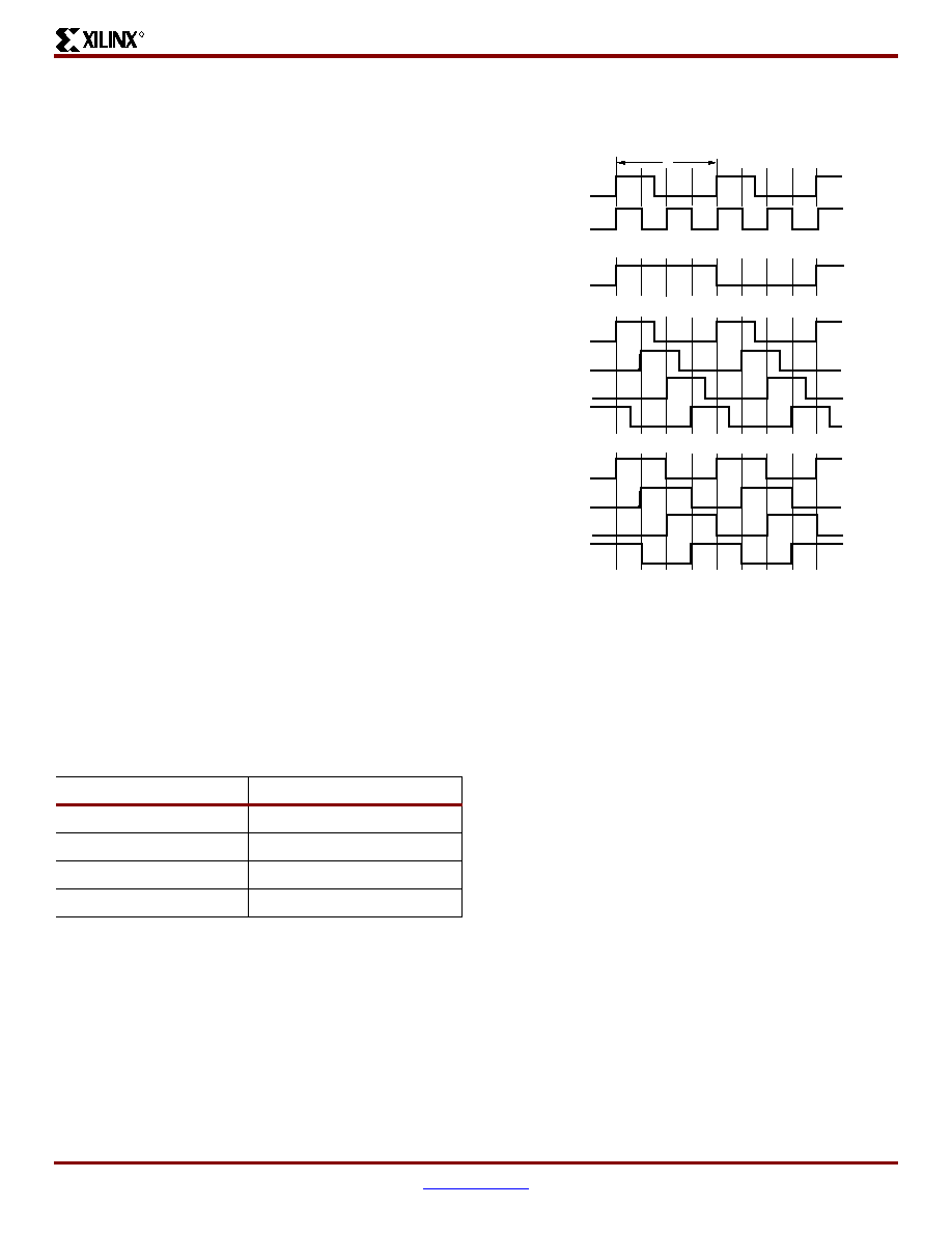
and the corresponding period shift appears in Table 13.
The timing diagrams in Figure 25 illustrate the DLL clock
output characteristics.
The DLL provides duty cycle correction on all 1x clock out-
puts such that all 1x clock outputs by default have a 50/50
duty cycle. The DUTY_CYCLE_CORRECTION property
(TRUE by default), controls this feature. In order to deacti-
vate
the
DLL
duty
cycle
correction,
attach
the
DUTY_CYCLE_CORRECTION=FALSE property to the
DLL symbol. When duty cycle correction deactivates, the
output clock has the same duty cycle as the source clock.
The DLL clock outputs can drive an OBUF, a BUFG, or they
can route directly to destination clock pins. The DLL clock
outputs can only drive the BUFGs that reside on the same
edge (top or bottom).
Locked Output — LOCKED
To achieve lock, the DLL might need to sample several thou-
sand clock cycles. After the DLL achieves lock, the
LOCKED signal activates. The DLL timing parameter sec-
tion of the data sheet provides estimates for locking times.
To guarantee that the system clock is established prior to
the device “waking up,” the DLL can delay the completion of
the device configuration process until after the DLL locks.
The STARTUP_WAIT property activates this feature.
Until the LOCKED signal activates, the DLL output clocks
are not valid and can exhibit glitches, spikes, or other spuri-
ous movement. In particular the CLK2X output appears as a
1x clock with a 25/75 duty cycle.
Table 13: Relationship of Phase-Shifted Output Clock
to Period Shift
Phase (degrees)
Period Shift (percent)
00%
90
25%
180
50%
270
75%
Figure 25: DLL Output Characteristics
ds022_29_121099
CLKIN
CLK2X
CLK0
CLK90
CLK180
CLK270
CLKDV
CLKDV_DIVIDE=2
DUTY_CYCLE_CORRECTION=FALSE
CLK0
CLK90
CLK180
CLK270
DUTY_CYCLE_CORRECTION=TRUE
t
0
90 180 270
0
90 180 270
相关PDF资料 |
PDF描述 |
|---|---|
| 748558-4 | CONN D-SUB FEMALE SCREW LOCK |
| XCV300E-7FG256I | IC FPGA 1.8V I-TEMP 256-FBGA |
| XCV300E-7BG352I | IC FPGA 1.8V I-TEMP 352-MBGA |
| HMC43DRAH | CONN EDGECARD 86POS R/A .100 SLD |
| XCV400E-7PQ240C | IC FPGA 1.8V C-TEMP 240-PQFP |
相关代理商/技术参数 |
参数描述 |
|---|---|
| XCV300E-8BG352I | 制造商:XILINX 制造商全称:XILINX 功能描述:Virtex-E 1.8 V Field Programmable Gate Arrays |
| XCV300E-8BG432C | 功能描述:IC FPGA 1.8V C-TEMP 432-MBGA RoHS:否 类别:集成电路 (IC) >> 嵌入式 - FPGA(现场可编程门阵列) 系列:Virtex®-E 产品变化通告:Step Intro and Pkg Change 11/March/2008 标准包装:1 系列:Virtex®-5 SXT LAB/CLB数:4080 逻辑元件/单元数:52224 RAM 位总计:4866048 输入/输出数:480 门数:- 电源电压:0.95 V ~ 1.05 V 安装类型:表面贴装 工作温度:-40°C ~ 100°C 封装/外壳:1136-BBGA,FCBGA 供应商设备封装:1136-FCBGA 配用:568-5088-ND - BOARD DEMO DAC1408D750122-1796-ND - EVALUATION PLATFORM VIRTEX-5 |
| XCV300E-8BG432C0773 | 制造商:Rochester Electronics LLC 功能描述: 制造商:Xilinx 功能描述: |
| XCV300E-8BG432I | 制造商:XILINX 制造商全称:XILINX 功能描述:Virtex-E 1.8 V Field Programmable Gate Arrays |
| XCV300E8BGG432C | 制造商:Xilinx 功能描述: |
发布紧急采购,3分钟左右您将得到回复。