参数资料
| 型号: | XCV400E-6PQ240C |
| 厂商: | Xilinx Inc |
| 文件页数: | 223/233页 |
| 文件大小: | 0K |
| 描述: | IC FPGA 1.8V C-TEMP 240-PQFP |
| 产品变化通告: | FPGA Family Discontinuation 18/Apr/2011 |
| 标准包装: | 24 |
| 系列: | Virtex®-E |
| LAB/CLB数: | 2400 |
| 逻辑元件/单元数: | 10800 |
| RAM 位总计: | 163840 |
| 输入/输出数: | 158 |
| 门数: | 569952 |
| 电源电压: | 1.71 V ~ 1.89 V |
| 安装类型: | 表面贴装 |
| 工作温度: | 0°C ~ 85°C |
| 封装/外壳: | 240-BFQFP |
| 供应商设备封装: | 240-PQFP(32x32) |
第1页第2页第3页第4页第5页第6页第7页第8页第9页第10页第11页第12页第13页第14页第15页第16页第17页第18页第19页第20页第21页第22页第23页第24页第25页第26页第27页第28页第29页第30页第31页第32页第33页第34页第35页第36页第37页第38页第39页第40页第41页第42页第43页第44页第45页第46页第47页第48页第49页第50页第51页第52页第53页第54页第55页第56页第57页第58页第59页第60页第61页第62页第63页第64页第65页第66页第67页第68页第69页第70页第71页第72页第73页第74页第75页第76页第77页第78页第79页第80页第81页第82页第83页第84页第85页第86页第87页第88页第89页第90页第91页第92页第93页第94页第95页第96页第97页第98页第99页第100页第101页第102页第103页第104页第105页第106页第107页第108页第109页第110页第111页第112页第113页第114页第115页第116页第117页第118页第119页第120页第121页第122页第123页第124页第125页第126页第127页第128页第129页第130页第131页第132页第133页第134页第135页第136页第137页第138页第139页第140页第141页第142页第143页第144页第145页第146页第147页第148页第149页第150页第151页第152页第153页第154页第155页第156页第157页第158页第159页第160页第161页第162页第163页第164页第165页第166页第167页第168页第169页第170页第171页第172页第173页第174页第175页第176页第177页第178页第179页第180页第181页第182页第183页第184页第185页第186页第187页第188页第189页第190页第191页第192页第193页第194页第195页第196页第197页第198页第199页第200页第201页第202页第203页第204页第205页第206页第207页第208页第209页第210页第211页第212页第213页第214页第215页第216页第217页第218页第219页第220页第221页第222页当前第223页第224页第225页第226页第227页第228页第229页第230页第231页第232页第233页
Virtex-E 1.8 V Field Programmable Gate Arrays
R
DS022-2 (v3.0) March 21, 2014
Module 2 of 4
Production Product Specification
3
— OBSOLETE — OBSOLETE — OBSOLETE — OBSOLETE —
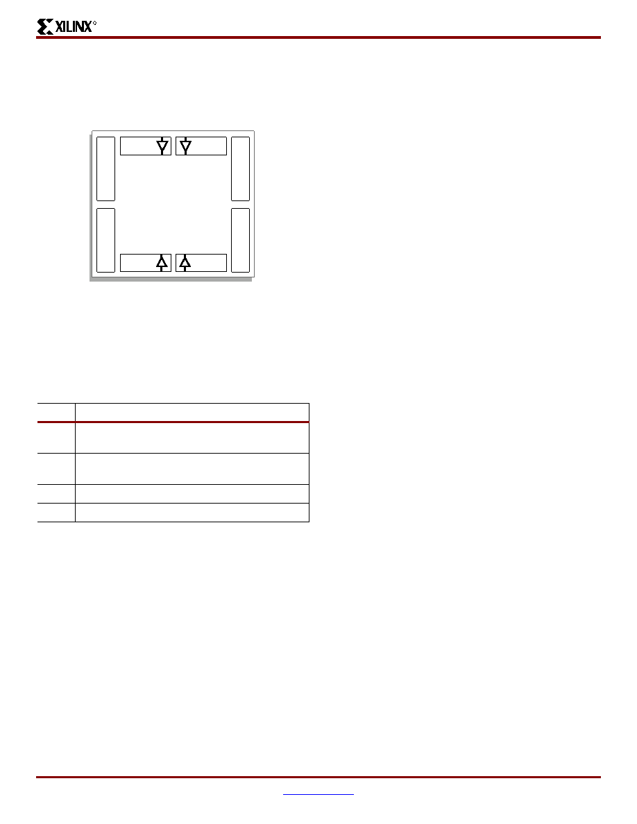
Eight I/O banks result from separating each edge of the
FPGA into two banks, as shown in Figure 3. Each bank has
multiple VCCO pins, all of which must be connected to the
same voltage. This voltage is determined by the output
standards in use.
Within a bank, output standards can be mixed only if they
use the same VCCO. Compatible standards are shown in
Table 2. GTL and GTL+ appear under all voltages because
their open-drain outputs do not depend on VCCO.
Some input standards require a user-supplied threshold
voltage, VREF. In this case, certain user-I/O pins are auto-
matically configured as inputs for the VREF voltage. Approx-
imately one in six of the I/O pins in the bank assume this
role.
The VREF pins within a bank are interconnected internally
and consequently only one VREF voltage can be used within
each bank. All VREF pins in the bank, however, must be con-
nected to the external voltage source for correct operation.
Within a bank, inputs that require VREF can be mixed with
those that do not. However, only one VREF voltage can be
used within a bank.
In
Virtex-E,
input
buffers
with
LVTTL,
LVCMOS2,
LVCMOS18, PCI33_3, PCI66_3 standards are supplied by
VCCO rather than VCCINT. For these standards, only input
and output buffers that have the same VCCO can be mixed
together.
The VCCO and VREF pins for each bank appear in the device
pin-out tables and diagrams. The diagrams also show the
bank affiliation of each I/O.
Within a given package, the number of VREF and VCCO pins
can vary depending on the size of device. In larger devices,
more I/O pins convert to VREF pins. Since these are always
a super set of the VREF pins used for smaller devices, it is
possible to design a PCB that permits migration to a larger
device if necessary. All the VREF pins for the largest device
anticipated must be connected to the VREF voltage, and not
used for I/O.
In smaller devices, some VCCO pins used in larger devices
do not connect within the package. These unconnected pins
can be left unconnected externally, or can be connected to
the VCCO voltage to permit migration to a larger device if
necessary.
Configurable Logic Blocks
The basic building block of the Virtex-E CLB is the logic cell
(LC). An LC includes a 4-input function generator, carry
logic, and a storage element. The output from the function
generator in each LC drives both the CLB output and the D
input of the flip-flop. Each Virtex-E CLB contains four LCs,
organized in two similar slices, as shown in Figure 4.
Figure 5 shows a more detailed view of a single slice.
In addition to the four basic LCs, the Virtex-E CLB contains
logic that combines function generators to provide functions
of five or six inputs. Consequently, when estimating the
number of system gates provided by a given device, each
CLB counts as 4.5 LCs.
Look-Up Tables
Virtex-E function generators are implemented as 4-input
look-up tables (LUTs). In addition to operating as a function
generator, each LUT can provide a 16 x 1-bit synchronous
RAM. Furthermore, the two LUTs within a slice can be com-
bined to create a 16 x 2-bit or 32 x 1-bit synchronous RAM,
or a 16 x 1-bit dual-port synchronous RAM.
The Virtex-E LUT can also provide a 16-bit shift register that
is ideal for capturing high-speed or burst-mode data. This
mode can also be used to store data in applications such as
Digital Signal Processing.
Figure 3: Virtex-E I/O Banks
Table 2: Compatible Output Standards
VCCO
Compatible Standards
3.3 V
PCI, LVTTL, SSTL3 I, SSTL3 II, CTT, AGP, GTL,
GTL+, LVPECL
2.5 V
SSTL2 I, SSTL2 II, LVCMOS2, GTL, GTL+,
BLVDS, LVDS
1.8 V
LVCMOS18, GTL, GTL+
1.5 V
HSTL I, HSTL III, HSTL IV, GTL, GTL+
ds022_03_121799
Bank 0
GCLK3 GCLK2
GCLK1 GCLK0
Bank 1
Bank 5
Bank 4
VirtexE
Device
Bank
7
Bank
6
Bank
2
Bank
3
相关PDF资料 |
PDF描述 |
|---|---|
| XC5VLX30T-1FFG323C | IC FPGA VIRTEX-5LX 30K 323-FCBGA |
| XC6SLX150T-3FGG900I | IC FPGA SPARTAN 6 147K 900FGGBGA |
| XC4VSX25-10FFG668C | IC FPGA VIRTEX-4 SX 25K 668FCBGA |
| XC2V500-5FG456I | IC FPGA VIRTEX-II 456FGBGA |
| XC2V500-6FGG456C | IC FPGA VIRTEX-II 500K 456-FBGA |
相关代理商/技术参数 |
参数描述 |
|---|---|
| XCV400E-6PQ240C0773 | 制造商:Rochester Electronics LLC 功能描述: 制造商:Xilinx 功能描述: |
| XCV400E-6PQ240I | 功能描述:IC FPGA 1.8V I-TEMP 240-PQFP RoHS:否 类别:集成电路 (IC) >> 嵌入式 - FPGA(现场可编程门阵列) 系列:Virtex®-E 产品变化通告:Step Intro and Pkg Change 11/March/2008 标准包装:1 系列:Virtex®-5 SXT LAB/CLB数:4080 逻辑元件/单元数:52224 RAM 位总计:4866048 输入/输出数:480 门数:- 电源电压:0.95 V ~ 1.05 V 安装类型:表面贴装 工作温度:-40°C ~ 100°C 封装/外壳:1136-BBGA,FCBGA 供应商设备封装:1136-FCBGA 配用:568-5088-ND - BOARD DEMO DAC1408D750122-1796-ND - EVALUATION PLATFORM VIRTEX-5 |
| XCV400E-6PQG240C | 制造商:Xilinx 功能描述:FPGA VIRTEX-E 129.6K GATES 10800 CELLS 357MHZ 0.18UM 1.8V 24 - Trays |
| XCV400E-7BG240C | 制造商:XILINX 制造商全称:XILINX 功能描述:Virtex⑩-E 1.8 V Field Programmable Gate Arrays |
| XCV400E-7BG240I | 制造商:XILINX 制造商全称:XILINX 功能描述:Virtex⑩-E 1.8 V Field Programmable Gate Arrays |
发布紧急采购,3分钟左右您将得到回复。