- 您现在的位置:买卖IC网 > PDF目录4059 > XPC8240LZU200E (Freescale Semiconductor)MCU HOST PROCESSOR 352-TBGA PDF资料下载
参数资料
| 型号: | XPC8240LZU200E |
| 厂商: | Freescale Semiconductor |
| 文件页数: | 3/8页 |
| 文件大小: | 0K |
| 描述: | MCU HOST PROCESSOR 352-TBGA |
| 标准包装: | 24 |
| 系列: | MPC82xx |
| 处理器类型: | 32-位 MPC82xx PowerQUICC II |
| 速度: | 200MHz |
| 电压: | 2.5V |
| 安装类型: | 表面贴装 |
| 封装/外壳: | 352-LBGA |
| 供应商设备封装: | 352-TBGA(35x35) |
| 包装: | 托盘 |
MPC8240 Part Number Specification for the XPC8240RXXnnnx Series
3
General Parameters
1.4.1.5 Power Characteristics
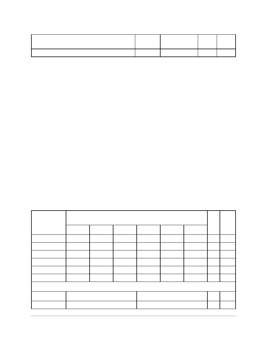
Table 5 provides power consumption data for the MPC8240. Power consumption on the PLL supply pins (AVDD
and AVDD2) and the DLL supply pin (LAVDD) less than 15 mW. This parameter is guaranteed by design and is not
tested.
Die-junction temperature
Tj
0 to 105
°C
Notes:
1. These are the recommended and tested operating conditions. Proper device operation outside of these conditions
is not guaranteed.
2. These signals are designed to withstand LVDD + 0.5 V DC when LVDD is connected to a 3.3- or 5.0-V DC power
supply.
3. LVDD input tolerant signals: PCI interface, EPIC control, and OSC_IN signals.
Cautions:
5. Input voltage (Vin) must not be greater than the supply voltage (VDD/AVDD/AVDD2/LAVDD) by more than 2.5 V at all
times, including during power-on reset.
6. OVDD must not exceed VDD/AVDD/AVDD2/LAVDD by more than 1.8 V at any time, including during power-on reset.
This limit may be exceeded for a maximum of 20 ms during power-on reset and power-down sequences.
7. VDD/AVDD/AVDD2/LAVDD must not exceed OVDD by more than 0.6 V at any time, including during power-on reset.
This limit may be exceeded for a maximum of 20 ms during power-on reset and power-down sequences.
8. GVDD must not exceed VDD/AVDD/AVDD2/LAVDD by more than 1.8 V at any time, including during power-on reset.
This limit may be exceeded for a maximum of 20 ms during power-on reset and power-down sequences.
9. LVDD must not exceed VDD/AVDD/AVDD2/LAVDD by more than 5.4 V at any time, including during power-on reset.
This limit may be exceeded for a maximum of 20 ms during power-on reset and power-down sequences.
10.LVDD must not exceed OVDD by more than 3.6 V at any time, including during power-on reset. This limit may be
exceeded for a maximum of 20 ms during power-on reset and power-down sequences.
Table 5. Preliminary Power Consumption
Mode
PCI Bus Clock/Memory Bus Clock
CPU Clock Frequency (MHz)
Unit
Notes
33/66/233
33/83/250
33/100/200
33/100/250
66/100/200
66/100/250
Typical
3.4
3.6
3.2
3.7
3.2
3.8
W
1, 5
Maximum—FP
3.8
4.1
3.6
4.2
3.6
4.3
W
1, 2
Maximum—INT
3.4
3.7
3.3
3.8
3.4
3.8
W
1, 3
Doze
2.2
2.4
2.2
2.6
2.2
2.6
W
1, 4, 6
Nap
700
800
900
mW
1, 4, 6
Sleep
500
800
mW
1, 4, 6
I/O Power Supplies
Mode
Minimum
Maximum
Unit
Notes
Typical—OVDD
200
600
mW
7, 8
Table 2. Recommended Operating Conditions (continued)
Characteristic
Symbol
Recommended
Value
Unit
Notes
F
re
e
sc
a
le
S
e
m
ic
o
n
d
u
c
to
r,
I
Freescale Semiconductor, Inc.
For More Information On This Product,
Go to: www.freescale.com
n
c
..
.
相关PDF资料 |
PDF描述 |
|---|---|
| MPC862PZQ50B | IC MPU PWRQUICC 50MHZ 357-PBGA |
| MPC862PVR50B | IC MPU POWERQUICC 50MHZ 357PBGA |
| FMC26DREI | CONN EDGECARD 52POS .100 EYELET |
| MPC8270CZUQLDA | IC MPU POWERQUICC II 480-TBGA |
| MPC8349CZUAJDB | IC MPU POWERQUICC II PRO 672TBGA |
相关代理商/技术参数 |
参数描述 |
|---|---|
| XPC8240RVV250 | 制造商:FREESCALE 制造商全称:Freescale Semiconductor, Inc 功能描述:Modified voltage specifications to achieve 250 MHz |
| XPC8240RVV250E | 功能描述:微处理器 - MPU INTEGRATED HOST PROC RoHS:否 制造商:Atmel 处理器系列:SAMA5D31 核心:ARM Cortex A5 数据总线宽度:32 bit 最大时钟频率:536 MHz 程序存储器大小:32 KB 数据 RAM 大小:128 KB 接口类型:CAN, Ethernet, LIN, SPI,TWI, UART, USB 工作电源电压:1.8 V to 3.3 V 最大工作温度:+ 85 C 安装风格:SMD/SMT 封装 / 箱体:FBGA-324 |
| XPC8240RZU250 | 制造商:FREESCALE 制造商全称:Freescale Semiconductor, Inc 功能描述:Modified voltage specifications to achieve 250 MHz |
| XPC8240RZU250E | 功能描述:微处理器 - MPU INTEGRATED HOST PROC RoHS:否 制造商:Atmel 处理器系列:SAMA5D31 核心:ARM Cortex A5 数据总线宽度:32 bit 最大时钟频率:536 MHz 程序存储器大小:32 KB 数据 RAM 大小:128 KB 接口类型:CAN, Ethernet, LIN, SPI,TWI, UART, USB 工作电源电压:1.8 V to 3.3 V 最大工作温度:+ 85 C 安装风格:SMD/SMT 封装 / 箱体:FBGA-324 |
| XPC8241LZP166 | 制造商:未知厂家 制造商全称:未知厂家 功能描述:Microprocessor |
发布紧急采购,3分钟左右您将得到回复。