- 您现在的位置:买卖IC网 > PDF目录225574 > XR1005 RF/MICROWAVE DOWN CONVERTER PDF资料下载
参数资料
| 型号: | XR1005 |
| 元件分类: | 上/下变频器 |
| 英文描述: | RF/MICROWAVE DOWN CONVERTER |
| 封装: | DIE-10 |
| 文件页数: | 1/7页 |
| 文件大小: | 402K |
| 代理商: | XR1005 |
Mimix Broadband, Inc., 10795 Rockley Rd., Houston, Texas 77099
Tel: 281.988.4600 Fax: 281.988.4615 mimixbroadband.com
Characteristic Data and Specifications are subject to change without notice.
2005 Mimix Broadband, Inc.
Export of this item may require appropriate export licensing from the U.S. Government. In purchasing these parts, U.S. Domestic customers accept
their obligation to be compliant with U.S. Export Laws.
May 2005 - Rev 13-May-05
Mimix Broadband
’s 19.0-26.0 GHz GaAs MMIC receiver has a noise
figure of 2.5 dB and 20.0 dB image rejection across the band. This
device is a two stage balanced LNA followed by an image reject sub-
harmonic anti-parallel diode mixer and includes an integrated LO
buffer amplifer. The image reject mixer eliminates the need for a
bandpass filter after the LNA to remove thermal noise at the image
frequency. The use of a sub-harmonic mixer makes the provision of
the LO easier than for fundamental mixers at these frequencies. I and Q
mixer outputs are provided and an external 90 degree hybrid is
required to select the desired sideband. This MMIC uses Mimix
Broadband
’s 0.15 m GaAs PHEMT device model technology, and is
based upon electron beam lithography to ensure high repeatability
and uniformity. The chip has surface passivation to protect and provide
a rugged part with backside via holes and gold metallization to allow
either a conductive epoxy or eutectic solder die attach process. This
device is well suited for Millimeter-wave Point-to-Point Radio, LMDS,
SATCOM and VSAT applications.
19.0-26.0 GHz GaAs MMIC
Receiver
Page 1 of 7
Sub-harmonic Receiver
Integrated LNA, LO Buffer, Image Reject Mixer
+2.0 dBm LO Drive Level
2.5 dB Noise Figure
20.0 dB Image Rejection
100% On-Wafer RF, DC and Noise Figure Testing
100% Visual Inspection to MIL-STD-883 Method 2010
Features
General Description
Absolute Maximum Ratings
Supply Voltage (Vd)
Supply Current (Id1,Id2)
Gate Bias Voltage (Vg)
Input Power (RF Pin)
Storage Temperature (Tstg)
Operating Temperature (Ta)
Channel Temperature (Tch)
+4.5 VDC
180, 165 mA
+0.3 VDC
0.0 dBm
-65 to +165 OC
-55 to MTTF Table
MTTF Table
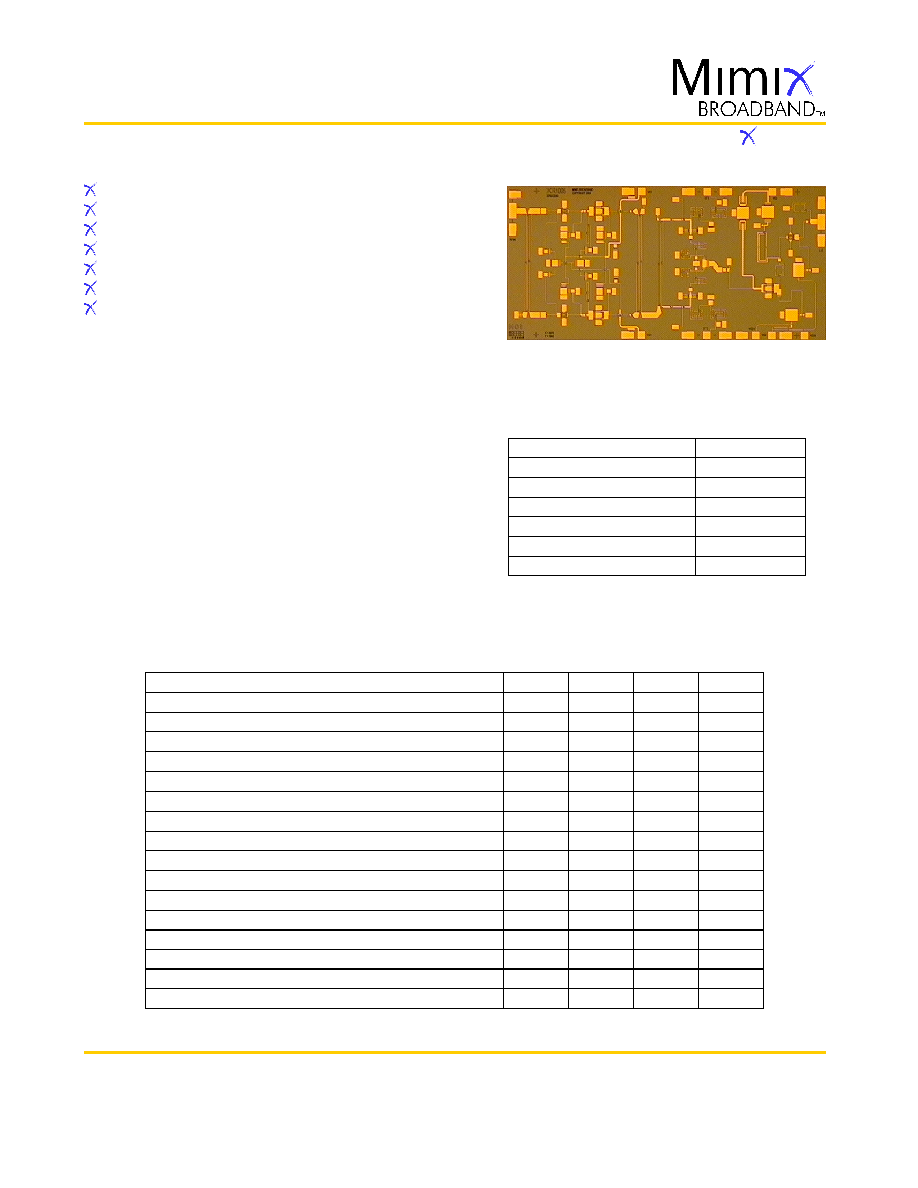
Chip Device Layout
(3) Channel temperature affects a device's MTTF. It is
recommended to keep channel temperature as low as
possible for maximum life.
3
Electrical Characteristics (AmbientTemperatureT = 25o C)
Units
GHz
dB
dBm
dBc
dB
dBm
VDC
mA
Min.
19.0
8.0
DC
-
-1.2
-
Typ.
-
12.0
8.0
+2.0
20.0
2.5
40.0
-7.0
+3.5
+4.0
-0.3
130
116
Max.
26.0
14.5
3.0
-
+4.5
+0.1
155
140
Parameter
Frequency Range (RF) Upper Side Band
Frequency Range (RF) Lower Side Band
Frequency Range (LO)
Frequency Range (IF)
Input Return Loss RF (S11)
Small Signal Conversion Gain RF/IF (S21)
LO Input Drive (PLO)
Image Rejection
Noise Figure (NF)
Isolation LO/RF @ LOx1/LOx2
Input Third Order Intercept (IIP3)
Drain Bias Voltage (Vd1)
Drain Bias Voltage (Vd2)
Gate Bias Voltage (Vg1,2)
Supply Current (Id1) (Vd1=3.5V, Vg=-0.3V Typical)
Supply Current (Id2) (Vd2=4.0V,Vg=-0.3V Typical)
(1) Measured using constant current.
(2) Measured using LO Input drive level of +2.0 dBm.
1,2
2
R1005
相关PDF资料 |
PDF描述 |
|---|---|
| XT38T32.768KHZE2 | QUARTZ CRYSTAL RESONATOR, 0.032768 MHz |
| XTL1021-1 | QUARTZ CRYSTAL RESONATOR, 16 MHz |
| XTL1022 | QUARTZ CRYSTAL RESONATOR, 24 MHz |
| XU1003-BD-000V | 19000 MHz - 26000 MHz RF/MICROWAVE UP CONVERTER |
| X | FEMALE, STRAIGHT TWO PART BOARD CONNECTOR, SOLDER |
相关代理商/技术参数 |
参数描述 |
|---|---|
| XR-1005CN | 制造商:未知厂家 制造商全称:未知厂家 功能描述:Analog Filter |
| XR-1005CP | 制造商:未知厂家 制造商全称:未知厂家 功能描述:Analog Filter |
| XR1005D | 制造商:未知厂家 制造商全称:未知厂家 功能描述:Analog Filter |
| XR1005-QD | 制造商:MIMIX 制造商全称:MIMIX 功能描述:19.0-26.0 GHz GaAs Receiver QFN, 7x7 mm |
| XR1005-QD_07 | 制造商:MIMIX 制造商全称:MIMIX 功能描述:19.0-26.0 GHz GaAs Receiver QFN, 7x7 mm |
发布紧急采购,3分钟左右您将得到回复。