- 您现在的位置:买卖IC网 > PDF目录11006 > XR2211ACP-F (Exar Corporation)IC FSK DEMOD/TONE DECOD 14PDIP PDF资料下载
参数资料
| 型号: | XR2211ACP-F |
| 厂商: | Exar Corporation |
| 文件页数: | 8/24页 |
| 文件大小: | 0K |
| 描述: | IC FSK DEMOD/TONE DECOD 14PDIP |
| 标准包装: | 25 |
| 功能: | FSK 解调器,音频解码器 |
| 电源电压: | 4.5 V ~ 20 V |
| 电流 - 电源: | 5mA |
| 功率(瓦特): | 900mW |
| 工作温度: | 0°C ~ 70°C |
| 安装类型: | 通孔 |
| 封装/外壳: | 14-DIP(0.300",7.62mm) |
| 供应商设备封装: | 14-PDIP |
| 包装: | 管件 |
| 包括: | 载波检测 |
| 其它名称: | 1016-1309-5 |

XR-2211A
16
Rev. 1.04
Design Instructions:
The circuit of
Figure 12 can be optimized for any tone detection application by the choice of the 5 key circuit components:
R0, R1, C0, C1 and CD. For a given input, the tone frequency, fS, these parameters are calculated as follows:
(All resistance in
W’s, all frequency in Hz and all capacitance in farads, unless otherwise specified)
a) Choose value of timing resistor R0 to be in the range of 10KW to 50KW. This choice is dictated by the max./min.
current that the internal voltage reference can deliver. The recommended value is R0 = 20KW. The final value of R0
is normally fine-tuned with the series potentiometer, RX.
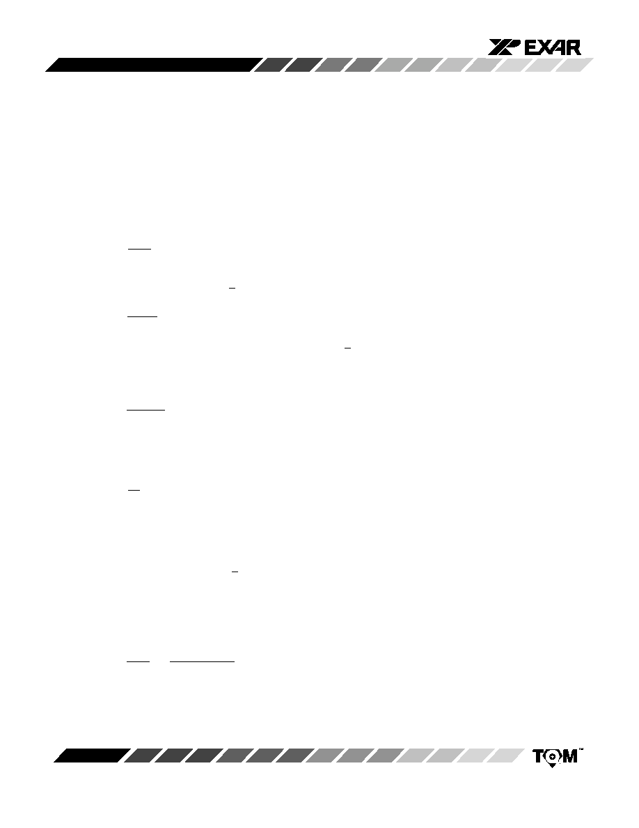
b) Calculate value of C0 from design equation (1) or from Figure 7 fS = fO:
C
O +
1
R
0fs
c)
Calculate R1 to set the bandwidth +Df (See design equation 5):
R
1
+
R
0f02
Df
Note: The total detection bandwidth covers the frequency range of fO +Df
d) Calculate value of C1 for a given loop damping factor:
Normally,
j = 0.5 is recommended.
C
1
+
1250
C
0
R
1
j2
Increasing C1 improves the out-of-band signal rejection, but increases the PLL capture time.
e) Calculate value of the filter capacitor CD . To avoid chatter at the logic output, with RD = 470KW, CD must be:
C
D
§ 16
Df
Cin
mF
Increasing CD slows down the logic output response time.
Design Examples:
Tone detector with a detection band of + 100Hz:
a) Choose value of timing resistor R0 to be in the range of 10KW to 50KW. This choice is dictated by the max./min.
current that the internal voltage reference can deliver. The recommended value is R0 = 20 KW. The final value of R0
is normally fine-tuned with the series potentiometer, RX.
b) Calculate value of C0 from design equation (1) or from Figure 6 fS = fO:
C
0
+ 1
R
0fS
+
1
20, 0001, 000
+ 50nF
相关PDF资料 |
PDF描述 |
|---|---|
| VE-BVY-IX-F3 | CONVERTER MOD DC/DC 3.3V 49.5W |
| VI-B2X-IY-B1 | CONVERTER MOD DC/DC 5.2V 50W |
| VI-B2T-IY-B1 | CONVERTER MOD DC/DC 6.5V 50W |
| VE-BVY-IX-F2 | CONVERTER MOD DC/DC 3.3V 49.5W |
| VI-B2R-IY-B1 | CONVERTER MOD DC/DC 7.5V 50W |
相关代理商/技术参数 |
参数描述 |
|---|---|
| XR2211ACP-F | 制造商:Exar Corporation 功能描述:IC DEMODULATOR/DECODER FSK 2211 |
| XR2211ACP-F | 制造商:Exar Corporation 功能描述:FSK Demodulator/ Tone Decoder IC |
| XR-2211CN | 制造商:未知厂家 制造商全称:未知厂家 功能描述:ASK/FSK Demodulator |
| XR2211CP | 制造商:EXAR 制造商全称:EXAR 功能描述: |
| XR-2211CP | 制造商:未知厂家 制造商全称:未知厂家 功能描述:ASK/FSK Demodulator |
发布紧急采购,3分钟左右您将得到回复。