- 您现在的位置:买卖IC网 > PDF目录10561 > XRT5997ES (Exar Corporation)IC LIU E1 7CH 3.3V 100TQFP PDF资料下载
参数资料
| 型号: | XRT5997ES |
| 厂商: | Exar Corporation |
| 文件页数: | 22/37页 |
| 文件大小: | 0K |
| 描述: | IC LIU E1 7CH 3.3V 100TQFP |
| 标准包装: | 1 |
| 类型: | 线路接口装置(LIU) |
| 驱动器/接收器数: | 7/7 |
| 规程: | E1 |
| 电源电压: | 3.14 V ~ 3.47 V |
| 安装类型: | 表面贴装 |
| 封装/外壳: | 100-LQFP |
| 供应商设备封装: | 100-TQFP(14x14) |
| 包装: | 托盘 |
| 其它名称: | 1016-1438 |
第1页第2页第3页第4页第5页第6页第7页第8页第9页第10页第11页第12页第13页第14页第15页第16页第17页第18页第19页第20页第21页当前第22页第23页第24页第25页第26页第27页第28页第29页第30页第31页第32页第33页第34页第35页第36页第37页
XRT5997
29
Rev. 1.0.0
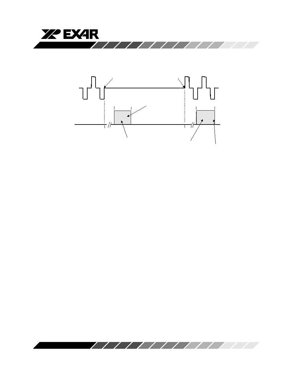
A ctual O ccurrence
of LO S C o ndition
Line S igna l
is R e stored
T im e R ang e fo r
LO S D e cla ratio n
T im e R ang e fo r
LO S C learance
G .775 C o m p liance
0 U I
10 U I
0 U I
10 U I
255 U I
255
UI
RxIN
L O S O u tp ut Pin
Note: F o r E 1 , 1 U I = 488ns
Figure 11. The Behavior of the LOS Output Indicator, in response to
the Loss of Signal, and the Restoration of the Signal
2.3 The “Receive Output Interface” block
The purpose of the “Receive Output Interface” block is
to interface directly with the “Receiving Terminal Equip-
ment”. The “Receive Output Interface” block outputs
the data (which has been recovered from the incoming
line signal) to the “Receive Terminal Equipment” via the
“RxPOS_x and RxNEG_x output pins.
If the “Receive Sections” of the XRT5997 device has
received a “Positive-Polarity” pulse, via the RTIP_x
and RRing_x input pins, then the Receive Output
Interface will output a pulse via the “RxPOS_x” output
pins.
Similarly, if the “Receive Sections” of the XRT5997
device has received a “Negative-Polarity” pulse, via the
RTIP_x and RRing_x input pins, then the Receive
Output Interface will output a pulse via the “RxNEG_x”
output pins.
Note:
The “Receive Output Interface” block does not
supply a recovered clock. This device is intended to be
used in those applications, where the “Clock Recovery”
circuit is realized in an ASIC solution.
3.0 Shutting off the Transmitter
Each channel (within the XRT5997 device) permits the
user to shut off the “Transmit Driver” within their
respective “Transmit Section”. This feature can come
in handy for system redundancy design considerations
or during diagnostic testing. The user can activate this
feature by either of the following ways.
Method 1:
Connect the Transmit Data input pins (e.g., TxPOS_x
and TxNEG_x) to a logic “1”; or allow them to float.
(These input pins have an internal “pull-up” resistor).
Method 2:
Connect the “TxClk_x” input pin to a logic “0” (e.g.,
GND) and continue to apply data via the TxPOS_x and
TxNEG_x input pins.
相关PDF资料 |
PDF描述 |
|---|---|
| XRT83VSH316IB-F | IC LIU SH T1/E1/J1 16CH 316STBGA |
| AD7685CCPZRL7 | IC ADC 16BIT SAR 250KSPS 10LFCSP |
| XRT91L32IQ-F | IC TXRX SONET/SDH 8BIT 100QFP |
| XRT91L30IQ-F | IC TXRX SONET/SDH 8BIT 64QFP |
| VI-BTF-MX-F1 | CONVERTER MOD DC/DC 72V 75W |
相关代理商/技术参数 |
参数描述 |
|---|---|
| XRT5997IV | 制造商:未知厂家 制造商全称:未知厂家 功能描述:PCM Transceiver |
| XRT5997IV-F | 功能描述:外围驱动器与原件 - PCI 3.3V or 5V 7-ch E1 temp -45 to 85C RoHS:否 制造商:PLX Technology 工作电源电压: 最大工作温度: 安装风格:SMD/SMT 封装 / 箱体:FCBGA-1156 封装:Tray |
| XRT5997IVTR-F | 功能描述:外围驱动器与原件 - PCI 7 Ch. E1 LIU RoHS:否 制造商:PLX Technology 工作电源电压: 最大工作温度: 安装风格:SMD/SMT 封装 / 箱体:FCBGA-1156 封装:Tray |
| XRT59L81IG-F | 功能描述:时钟发生器及支持产品 BITS Clock Generator RoHS:否 制造商:Silicon Labs 类型:Clock Generators 最大输入频率:14.318 MHz 最大输出频率:166 MHz 输出端数量:16 占空比 - 最大:55 % 工作电源电压:3.3 V 工作电源电流:1 mA 最大工作温度:+ 85 C 安装风格:SMD/SMT 封装 / 箱体:QFN-56 |
| XRT59L81IGTR-F | 功能描述:时钟发生器及支持产品 BITS Clock Generator RoHS:否 制造商:Silicon Labs 类型:Clock Generators 最大输入频率:14.318 MHz 最大输出频率:166 MHz 输出端数量:16 占空比 - 最大:55 % 工作电源电压:3.3 V 工作电源电流:1 mA 最大工作温度:+ 85 C 安装风格:SMD/SMT 封装 / 箱体:QFN-56 |
发布紧急采购,3分钟左右您将得到回复。