- 您现在的位置:买卖IC网 > PDF目录10563 > XRT83D10IW-F (Exar Corporation)IC LIU T1/E1 SGL 28SOJ PDF资料下载
参数资料
| 型号: | XRT83D10IW-F |
| 厂商: | Exar Corporation |
| 文件页数: | 6/18页 |
| 文件大小: | 0K |
| 描述: | IC LIU T1/E1 SGL 28SOJ |
| 标准包装: | 27 |
| 类型: | 线路接口装置(LIU) |
| 驱动器/接收器数: | 1/1 |
| 规程: | T1,E1 |
| 电源电压: | 3.135 V ~ 3.465 V |
| 安装类型: | 表面贴装 |
| 封装/外壳: | 28-BSOJ |
| 供应商设备封装: | 28-SOJ |
| 包装: | 管件 |
| 其它名称: | 1016-1581-5 XRT83D10IW-F-ND |
XRT83D10
xr
SINGLE CHANNEL DS1/CEPT LINE INTERFACE UNIT
REV. 1.0.3
14
initiated, an all 1s signal is sent to the network and does not corrupt the looped data. The RLOS alarm still
monitors the entire receive function.
A remote loopback (LP2) loops the recovered clock and re-timed data into the transmitter and back onto the
line. The receive front end, receive PLL, jitter attenuator (if enabled), and transmit driver circuitry are all
exercised. The transmit clock, transmit data, and TAOS inputs are ignored. Valid receive output data continues
to be sent to RPDATA and RNDATA. This loop can be used to isolate failures between systems.
A digital local loopback (LP3) directly loops the transmit clock and data to the receive clock and data output
pins. The transmit all 1s signal can be transmitted when in this loopback. LP3 (rather than LP1) must be
selected if MODE2 = 0.
1.6
MICROPROCESSOR INTERFACE:
A chip select input (CS) configures the device in either hardware mode or microprocessor mode. The chip-
select function, applies to the following inputs: MODE1, MODE2,EC1,EC2,EC3,LOOPA and LOOPB. In the
hardware mode, any change on these asynchronous input pins fed directly into the device.To maintain
hardware mode, set CS = 0. In the microprocessor mode, new digital control inputs are loaded into the
XRT83D10 on the falling edge of CS and are latched on the rising edge of CS.
1.7
IN-CIRCUIT TESTING:
The XRT83D10 has the ability to allow for in-circuit testing by activating the high-impedance mode (ICT =
0).During this mode, all output buffers (TTIP,TRING,RCLK,RPDATA,RNDATA,RLOS,FOFS and CLKLOS) are
3-stated. During the 3-stated condition, the absolute maximum voltage ratings must not be exceeded on any
pin.
1.8
ABSOLUTE MAXIMUM RATINGS:
Stresses in excess of absolute maximum ratings can cause permanent or latent damage to the device. These
are absolute stress ratings only.Functional operation of the device is not implied at these or any other
conditions in excess of those given in the operational sections of this data sheet.
NOTE:
Stresses in excess of the Absolute Maximum Ratings can cause permanent damage to the device.The above
values are absolute stress ratings only. Exposure to Absolute Maximum Ratings for extended periods can
adversely affect device reliability.
2.0
APPLICATIONS:
2.1
Line Termination:
For the following applications, the tolerance of all transformer turns ratios is a maximum of ± 2%. The tolerance
of all resistors in the transmit path is a maximum of ± 1%.
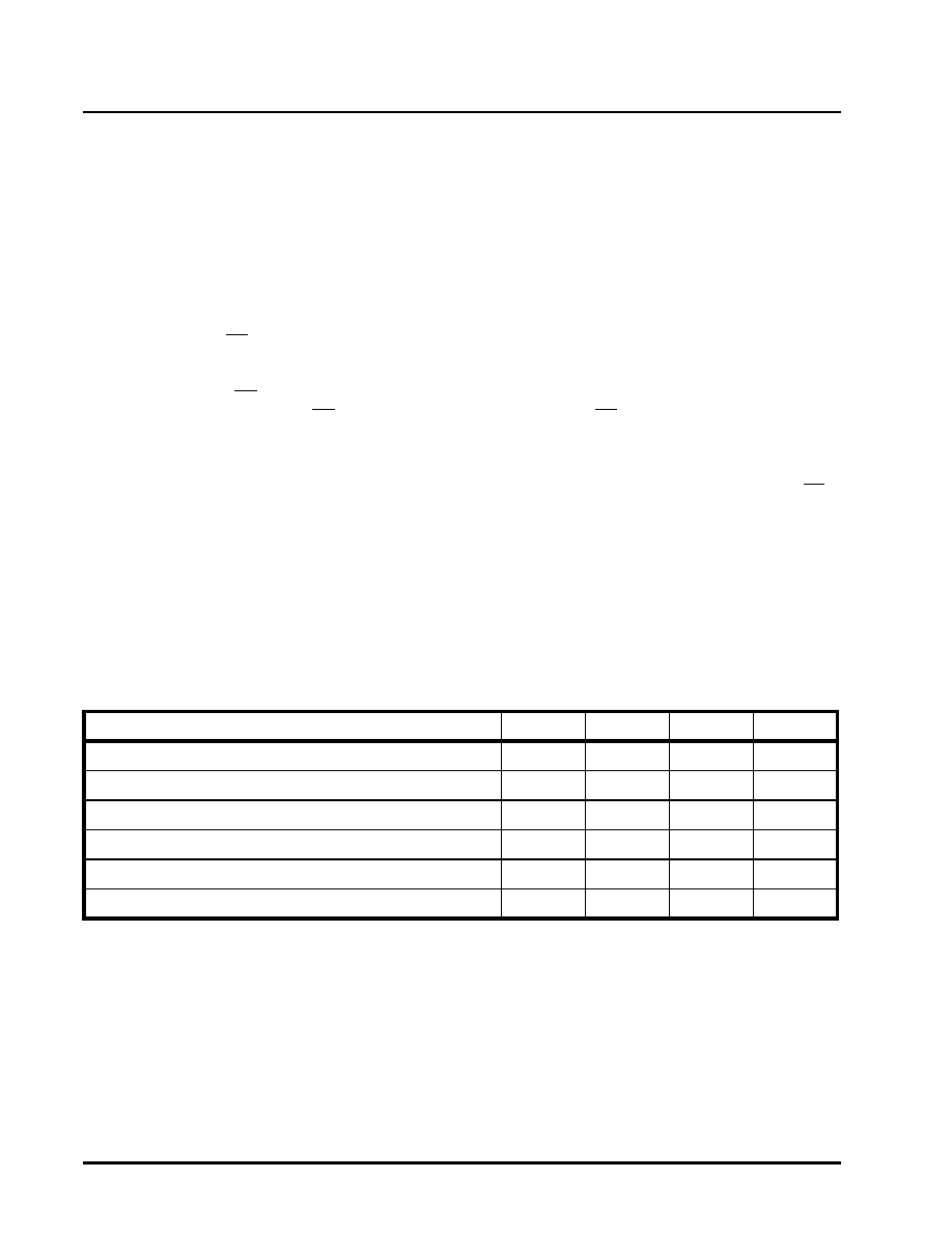
ELECTRICAL CHARACTERISTICS - ABSOLUTE MAXIMUM RATINGS
PARAMETER
SYMBOL
MIN
MAX
UNIT
DC Supply Voltage Range
VDD
-0.5
6.5
V
Storage Temperature
STO
-65
125
degC
Maximum Voltage (any pin) with respect to VDD
0.5
V
Minimum Voltage (any pin) with respect to GND
-0.5
V
Maximum voltage allowed (RTIP,RRING) with respect to GND
-5.0
5.0
V
ESD (Human-body model)
2000
V
相关PDF资料 |
PDF描述 |
|---|---|
| VI-J1Z-MW-F1 | CONVERTER MOD DC/DC 2V 40W |
| 206039-1 | CONN PLUG CPC 28POS REV SER 2 |
| 211769-3 | CONN RCPT CPC 9POS REV FREE HANG |
| VE-2TF-IW-F3 | CONVERTER MOD DC/DC 72V 100W |
| MAX1247BCPE+ | IC ADC SRL 4CH 12BIT 2.7V 16-DIP |
相关代理商/技术参数 |
参数描述 |
|---|---|
| XRT83D10IWTR | 功能描述:外围驱动器与原件 - PCI RoHS:否 制造商:PLX Technology 工作电源电压: 最大工作温度: 安装风格:SMD/SMT 封装 / 箱体:FCBGA-1156 封装:Tray |
| XRT83D10IWTR-F | 功能描述:外围驱动器与原件 - PCI RoHS:否 制造商:PLX Technology 工作电源电压: 最大工作温度: 安装风格:SMD/SMT 封装 / 箱体:FCBGA-1156 封装:Tray |
| XRT83L30 | 制造商:EXAR 制造商全称:EXAR 功能描述:SINGLE-CHANNEL T1/E1/J1 LH/SH TRANSCEIVER WITH CLOCK RECOVERY AND JITTER ATTENUATOR |
| XRT83L30_06 | 制造商:EXAR 制造商全称:EXAR 功能描述:SINGLE-CHANNEL T1/E1/J1 LH/SH TRANSCEIVER WITH CLOCK RECOVERY AND JITTER ATTENUATOR |
| XRT83L30ES | 功能描述:外围驱动器与原件 - PCI RoHS:否 制造商:PLX Technology 工作电源电压: 最大工作温度: 安装风格:SMD/SMT 封装 / 箱体:FCBGA-1156 封装:Tray |
发布紧急采购,3分钟左右您将得到回复。