- 您现在的位置:买卖IC网 > PDF目录297827 > XTR114UAE4 (TEXAS INSTRUMENTS INC) SPECIALTY ANALOG CIRCUIT, PDSO14 PDF资料下载
参数资料
| 型号: | XTR114UAE4 |
| 厂商: | TEXAS INSTRUMENTS INC |
| 元件分类: | 模拟信号调理 |
| 英文描述: | SPECIALTY ANALOG CIRCUIT, PDSO14 |
| 封装: | ROHS COMPLIANT, PLASTIC, SOIC-14 |
| 文件页数: | 18/18页 |
| 文件大小: | 211K |
| 代理商: | XTR114UAE4 |
9
XTR112, XTR114
range from 7.5V to 36V. The loop supply voltage, VPS, will
differ from the applied voltage according to the voltage drop
on the current sensing resistor, RL (plus any other voltage
drop in the line).
If a low loop supply voltage is used, RL (including the loop
wiring resistance) must be made a relatively low value to
assure that V+ remains 7.5V or greater for the maximum
loop current of 20mA:
It is recommended to design for V+ equal or greater than
7.5V with loop currents up to 30mA to allow for out-of-
range input conditions.
The low operating voltage (7.5V) of the XTR112 and
XTR114 allow operation directly from personal computer
power supplies (12V
±5%). When used with the RCV420
Current Loop Receiver (Figure 7), load resistor voltage drop
is limited to 3V.
ADJUSTING INITIAL ERRORS
Many applications require adjustment of initial errors. Input
offset and reference current mismatch errors can be cor-
rected by adjustment of the zero resistor, RZ. Adjusting the
gain-setting resistor, RG, corrects any errors associated with
gain.
TWO-WIRE AND THREE-WIRE RTD
CONNECTIONS
In Figure 1, the RTD can be located remotely simply by
extending the two connections to the RTD. With this remote
two-wire connection to the RTD, line resistance will intro-
duce error. This error can be partially corrected by adjusting
the values of RZ, RG, and RLIN1.
A better method for remotely located RTDs is the three-wire
RTD connection shown in Figure 3. This circuit offers
improved accuracy. RZ’s current is routed through a third
wire to the RTD. Assuming line resistance is equal in RTD
lines 1 and 2, this produces a small common-mode voltage
which is rejected by the XTR112 and XTR114. A second
resistor, RLIN2, is required for linearization.
Note that although the two-wire and three-wire RTD con-
nection circuits are very similar, the gain-setting resistor,
RG, has slightly different equations:
Two-wire:
Three-wire:
where RZ = RTD resistance at TMIN
R1 = RTD resistance at (TMIN + TMAX)/2
R2 = RTD resistance at TMAX
IREF = 0.25 for XTR112
IREF = 0.1 for XTR114
A negative input voltage, VIN, will cause the output current
to be less than 4mA. Increasingly negative VIN will cause the
output current to limit at approximately 1.3mA for the
XTR112 and 1mA for the XTR114. Refer to the typical
curve “Under-Scale Current vs Temperature.”
Increasingly positive input voltage (greater than the full-
scale input) will produce increasing output current according
to the transfer function, up to the output current limit of
approximately 27mA. Refer to the typical curve “Over-
Scale Current vs Temperature.”
EXTERNAL TRANSISTOR
Transistor Q1 conducts the majority of the signal-dependent
4-20mA loop current. Using an external transistor isolates
the majority of the power dissipation from the precision
input and reference circuitry of the XTR112 and XTR114,
maintaining excellent accuracy.
Since the external transistor is inside a feedback loop its
characteristics are not critical. Requirements are: VCEO =
45V min,
β = 40 min and P
D = 800mW. Power dissipation
requirements may be lower if the loop power supply voltage
is less than 36V. Some possible choices for Q1 are listed in
Figure 1.
The XTR112 and XTR114 can be operated without this
external transistor, however, accuracy will be somewhat
degraded due to the internal power dissipation. Operation
without Q1 is not recommended for extended temperature
ranges. A resistor (R = 3.3k
) connected between the I
RET
pin and the E (emitter) pin may be needed for operation
below 0
°C without Q
1 to guarantee the full 20mA full-scale
output, especially with V+ near 7.5V.
LOOP POWER SUPPLY
The voltage applied to the XTR112 and XTR114, V+, is
measured with respect to the IO connection, pin 7. V+ can
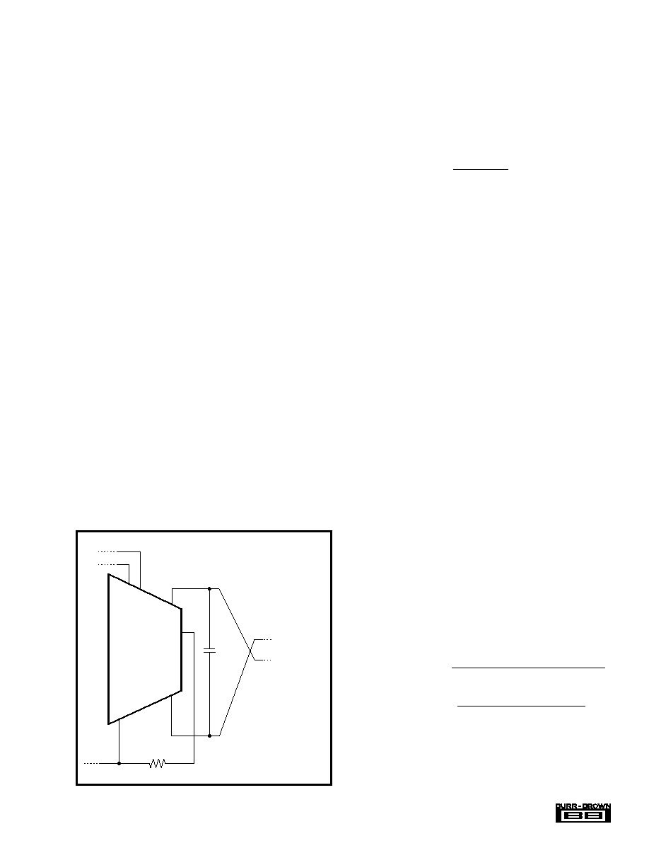
FIGURE 2. Operation Without External Transistor.
8
XTR112
XTR114
0.01
F
E
I
O
I
RET
V+
10
7
6
R
Q = 3.3k
For operation without external
transistor, connect a 3.3k
resistor between pin 6 and
pin 8. See text for discussion
of performance.
R
L max =
(V
+)– 7.5V
20mA
–R
WIRING
R
IR R
R
R R
RR
G
REF
Z
=
+
[]
25
2
12
2
21
.(
) – (
)
–
R
IR
R
RR
G
REF
Z
=
25
21
.(
–
)(
–
)
–
相关PDF资料 |
PDF描述 |
|---|---|
| XVT9007 | TCVCXO, CLIPPED SINE OUTPUT, 19.6608 MHz |
| XWD12129 | 2-OUTPUT 150 W DC-DC REG PWR SUPPLY MODULE |
| XWS1205-82H | 1-OUTPUT 150 W DC-DC REG PWR SUPPLY MODULE |
| XWS2415-HS | 1-OUTPUT DC-DC REG PWR SUPPLY MODULE |
| XWS2405-HS | 1-OUTPUT DC-DC REG PWR SUPPLY MODULE |
相关代理商/技术参数 |
参数描述 |
|---|---|
| XTR114UE4 | 功能描述:电流灵敏放大器 4-20mA Crnt Trnsmtr w/Sensor Exc & Lin RoHS:否 制造商:Texas Instruments 通道数量: 共模抑制比(最小值):110 dB 输入补偿电压:80 uV 电源电压-最大:5.5 V 电源电压-最小:2.7 V 电源电流:350 uA 最大工作温度:+ 125 C 最小工作温度:- 40 C 安装风格:SMD/SMT 封装 / 箱体:VQFN-16 封装:Reel |
| XTR115 | 制造商:BB 制造商全称:BB 功能描述:4-20mA CURRENT LOOP TRANSMITTERS |
| XTR115U | 功能描述:电流灵敏放大器 4-20mA Current Loop Transmitters RoHS:否 制造商:Texas Instruments 通道数量: 共模抑制比(最小值):110 dB 输入补偿电压:80 uV 电源电压-最大:5.5 V 电源电压-最小:2.7 V 电源电流:350 uA 最大工作温度:+ 125 C 最小工作温度:- 40 C 安装风格:SMD/SMT 封装 / 箱体:VQFN-16 封装:Reel |
| XTR115U | 制造商:Texas Instruments 功能描述:IC's |
| XTR115U | 制造商:Texas Instruments 功能描述:IC CURRENT LOOP TRANSMITTER SOIC8 |
发布紧急采购,3分钟左右您将得到回复。