- 您现在的位置:买卖IC网 > PDF目录48103 > YNL05S10009-001 (POWER-ONE INC) 1-OUTPUT DC-DC REG PWR SUPPLY MODULE PDF资料下载
参数资料
| 型号: | YNL05S10009-001 |
| 厂商: | POWER-ONE INC |
| 元件分类: | 电源模块 |
| 英文描述: | 1-OUTPUT DC-DC REG PWR SUPPLY MODULE |
| 封装: | ROHS COMPLIANT PACKAGE-6 |
| 文件页数: | 22/23页 |
| 文件大小: | 399K |
| 代理商: | YNL05S10009-001 |
FEB 17, 2006 revised to NOV 03, 2006
Page 8 of 23
www.power-one.com
YNL05S100xy DC-DC Converter Data Sheet
3.0 to 5.5 VDC Input; 0.9 to 3.3 VDC @ 10 A Output
The figures are numbered as Fig. x.y, where x
indicates the different output voltages, and y
associates with specific plots (y = 1 for the vertical
thermal derating, …). For example, Fig. x.1 will refer
to the vertical thermal derating for all the output
voltages in general.
The following pages contain specific plots or
waveforms associated with the converter. Additional
comments for specific data are provided below.
Test Conditions
All data presented were taken with the converter
soldered to a test board, specifically a 0.060” thick
printed wiring board (PWB) with four layers. The top
and bottom layers were not metalized. The two inner
layers, comprised of two-ounce copper, were used to
provide traces for connectivity to the converter.
The lack of metalization on the outer layers as well
as the limited thermal connection ensured that heat
transfer from the converter to the PWB was
minimized. This provides a worst-case but consistent
scenario for thermal derating purposes.
All measurements requiring airflow were made in the
vertical and horizontal wind tunnels using Infrared
(IR)
thermography
and
thermocouples
for
thermometry.
Ensuring components on the converter do not
exceed their ratings is important to maintaining high
reliability. If one anticipates operating the converter
at or close to the maximum loads specified in the
derating curves, it is prudent to check actual
operating
temperatures
in
the
application.
Thermographic
imaging
is
preferable;
if
this
capability is not available, then thermocouples may
be used. The use of AWG #40 gauge thermocouple
is recommended to ensure measurement accuracy.
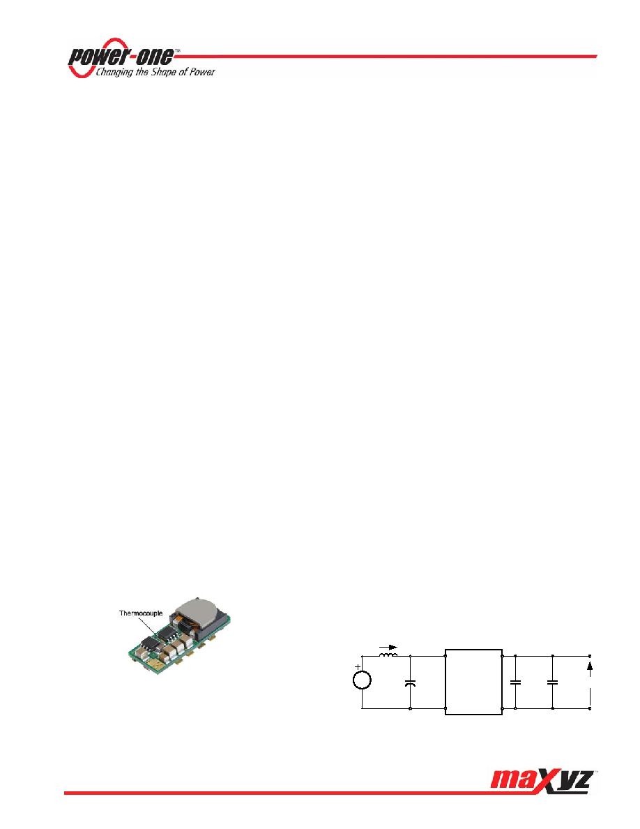
Careful routing of the thermocouple leads will further
minimize measurement error. Refer to Fig. G for the
optimum measuring thermocouple location.
Fig. G: Location of the thermocouple for thermal testing.
Thermal Derating
Load current vs. ambient temperature and airflow
rates are given in Figs. x.1 and Figs. x.2 for
maximum
temperature
of
110°C.
Ambient
temperature was varied between 25 °C and 85 °C,
with airflow rates from 30 to 500 LFM (0.15 m/s to
2.5 m/s), and vertical and horizontal mountings. The
airflow during the testing is parallel to the short axis
of the converter, going from pin 1 and pin 6 to
pins 2–5.
For each set of conditions, the maximum load
current is defined as the lowest of:
(i) The output current at which any MOSFET
temperature does not exceed a maximum specified
temperature
(110°C)
as
indicated
by
the
thermographic image, or
(ii) The maximum current rating of the converter
(10 A).
During normal operation, derating curves with
maximum FET temperature less than or equal to
110 °C should not be exceeded. Temperature on the
PCB at the thermocouple location shown in Fig. G
should not exceed 110 °C in order to operate inside
the derating curves.
Efficiency
Fig. x.3 shows the efficiency vs. load current plot for
ambient temperature of 25 C, airflow rate of
200 LFM (1 m/s), and input voltages of 4.5 V, 5.0 V,
and 5.5 V. Fig. x.4 is for input voltages of 3.0 V,
3.3 V, and 3.6 V, and for output voltages ≤ 2.5 V.
Power Dissipation
Fig. 3.3V.4 shows the power dissipation vs. load
current plot for Ta = 25 C, airflow rate of 200 LFM
(1 m/s) with vertical mounting and input voltages of
4.5 V, 5.0 V, and 5.5 V, and output of 3.3 V.
Ripple and Noise
The output voltage ripple waveform is measured at
full rated load current. Note that all output voltage
waveforms are measured across a 1 μF ceramic
capacitor.
The output voltage ripple and input reflected-ripple
current waveforms are obtained using the test setup
shown in Fig. H.
Vout
Vsource
1
μF
ceramic
capacitor
1
μH
source
inductance
DC-DC
Converter
4x47
μF
ceramic
capacitor
47
μF
ceramic
capacitor
CO
CIN
Y-Series
Fig. H: Test Setup for measuring input reflected-ripple
currents, is and output voltage ripple.
相关PDF资料 |
PDF描述 |
|---|---|
| YNL05S10015-D01 | 1-OUTPUT DC-DC REG PWR SUPPLY MODULE |
| YNL05S10033-D02G | 1-OUTPUT DC-DC REG PWR SUPPLY MODULE |
| YNL05S10033-002G | 1-OUTPUT DC-DC REG PWR SUPPLY MODULE |
| YNL05S10009-D01G | 1-OUTPUT DC-DC REG PWR SUPPLY MODULE |
| YNL05S10010-D01G | 1-OUTPUT DC-DC REG PWR SUPPLY MODULE |
相关代理商/技术参数 |
参数描述 |
|---|---|
| YNL05S10009-0G | 制造商:Power-One 功能描述:DC/DC PS SGL-OUT 0.9V 10A 33W 6SMD - Bulk |
| YNL05S10009-D | 制造商:Power-One 功能描述:DC/DC PS SGL-OUT 0.9V 10A 33W 6SMD - Bulk |
| YNL05S10009-DG | 制造商:Power-One 功能描述:DC/DC PS SGL-OUT 0.9V 10A 33W 6SMD - Bulk |
| YNL05S10010-0G | 制造商:Power-One 功能描述:DC/DC PS SGL-OUT 1V 10A 33W 6SMD - Bulk |
| YNL05S10010-D | 制造商:Power-One 功能描述:DC/DC PS SGL-OUT 1V 10A 33W 6SMD - Bulk |
发布紧急采购,3分钟左右您将得到回复。