- 您现在的位置:买卖IC网 > PDF目录15167 > ZL2008ALBFT1 (Intersil)IC REG CTRLR BUCK PWM VM 36-QFN PDF资料下载
参数资料
| 型号: | ZL2008ALBFT1 |
| 厂商: | Intersil |
| 文件页数: | 21/42页 |
| 文件大小: | 0K |
| 描述: | IC REG CTRLR BUCK PWM VM 36-QFN |
| 标准包装: | 1,000 |
| PWM 型: | 电压模式 |
| 输出数: | 1 |
| 频率 - 最大: | 1.4MHz |
| 占空比: | 95% |
| 电源电压: | 3 V ~ 5.5 V |
| 降压: | 是 |
| 升压: | 无 |
| 回扫: | 无 |
| 反相: | 无 |
| 倍增器: | 无 |
| 除法器: | 无 |
| Cuk: | 无 |
| 隔离: | 无 |
| 工作温度: | -40°C ~ 85°C |
| 封装/外壳: | 36-VFQFN 裸露焊盘 |
| 包装: | 带卷 (TR) |
第1页第2页第3页第4页第5页第6页第7页第8页第9页第10页第11页第12页第13页第14页第15页第16页第17页第18页第19页第20页当前第21页第22页第23页第24页第25页第26页第27页第28页第29页第30页第31页第32页第33页第34页第35页第36页第37页第38页第39页第40页第41页第42页
�� �
�
�ZL2008�
�D� (� V� IN� ?� max� ?� V� OUT� )� +� (� 1� ?� D� )� ?� V� OUT�
�=�
�R� 1� ?� min�
�C� L� (which� is� the� average� I� OUT� DCR� product)� is� small� and� can� be�
�neglected.� Therefore,� the� minimum� value� of� R� 1� may� be�
�approximated� Equation� 26:� ,�
�2� 2�
�(EQ.� 26)�
�P� R� 1� pkg� ?� max� ?� δ� P�
�ZL�
�GH�
�SW�
�ISENA�
�V� IN�
�V� OUT�
�GL�
�where� P� R1pkg-� max� is� the� maximum� power� dissipation�
�specification� for� the� resistor� package� and� P� is� the� derating� factor�
�for� the� same� parameter� (eg.:� P� R1pkg-� max� =� 0.0625W� for� 0603�
�package,� P� =� 50%� @� 85°C).� Once� R� 1-� min� has� been� calculated,�
��ISENB�
�MOSFET� R� DS(ON)� Sensing�
�V� IN�
�C� L� ?� max� =�
�L�
�(EQ.� 27)�
�R� 1� ?� min� ?� DCR�
�and� choose� the� next-lowest� readily� available� value� (e.g.:� For�
�C� L-� max� =� 1.86μF,� C� L� =� 1.5μF� is� a� good� choice).� Then� substitute�
�the� chosen� value� into� the� same� equation� and� re-calculate� the�
�value� of� R� 1� .� Choose� the� 1%� resistor� standard� value� closest� to� this�
�re-calculated� value� of� R� 1� .� The� error� due� to� the� mismatch� of� the�
�two� time� constants� is� expressed� in� Equation� 28:�
�GH�
�SW�
�ZL�
�GL�
�ISENA�
�ISENB�
�Inductor� DCR� Sensing�
�(V� OUT� must� be� less� than� 4.0� V)�
�V� OUT�
�R� 1� ?� C� L� ?� DCR� ?� ?�
�ε� τ� =� ?� ?� 1� ?�
�?� 100� %�
�?�
�R� 2� =� 5� ?� R� 1�
�?�
�(EQ.� 28)�
�?� L� avg� ?�
�The� value� of� R� 2� should� be� simply� five� times� that� of� R� 1� :�
�(EQ.� 29)�
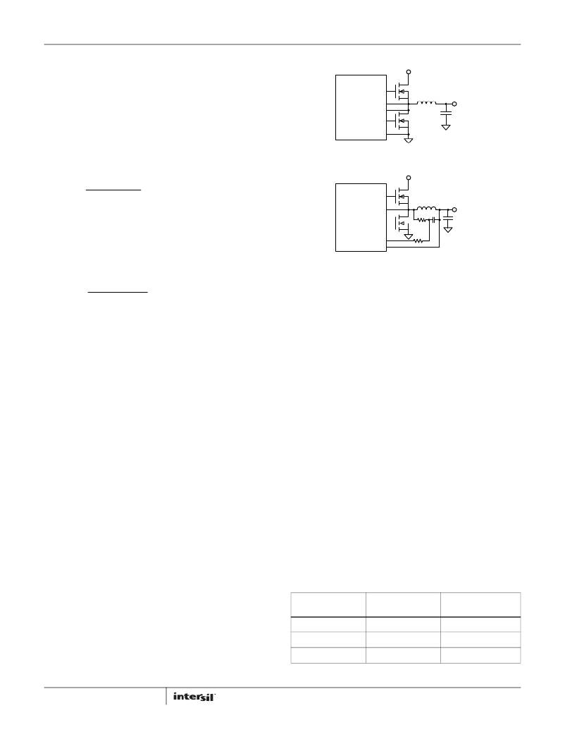
�For� the� R� DS(ON)� current� sensing� method,� the� external� low� side�
�MOSFET� will� act� as� the� sensing� element� as� indicated� in�
�Figure� 16.�
�Current� Limit� Threshold� Selection�
�It� is� recommended� that� the� user� include� a� current� limiting�
�mechanism� in� their� design� to� protect� the� power� supply� from�
�damage� and� prevent� excessive� current� from� being� drawn� from�
�the� input� supply� in� the� event� that� the� output� is� shorted� to� ground�
�or� an� overload� condition� is� imposed� on� the� output.� Current�
�limiting� is� accomplished� by� sensing� the� current� through� the�
�circuit� during� a� portion� of� the� duty� cycle.�
�Output� current� sensing� can� be� accomplished� by� measuring� the�
�voltage� across� a� series� resistive� sensing� element� according� to�
�Equation� 30:�
�FIGURE� 16.� Current� Sensing� Methods�
�To� set� the� current� limit� threshold,� the� user� must� first� select� a�
�current� sensing� method.� The� ZL2008� incorporates� two� methods�
�for� current� sensing,� synchronous� MOSFET� R� DS(ON)� sensing� and�
�inductor� DC� resistance� (DCR)� sensing;� Figure� 16� shows� a�
�simplified� schematic� for� each� method.� The� current� sensing�
�method� can� be� selected� using� the� CFG2� pin,� as� shown� in�
�Tables� 26� and� 28,� or� via� the� I� 2� C/SMBus� interface.� Please� refer� to�
�Application� Note� AN2033� for� details.�
�In� addition� to� selecting� the� current� sensing� method,� the� ZL2008�
�gives� the� power� supply� designer� several� choices� for� the� fault�
�response� during� over� or� under� current� condition.� The� user� can�
�select� the� number� of� violations� allowed� before� declaring� fault,� a�
�blanking� time� and� the� action� taken� when� a� fault� is� detected.�
�The� blanking� time� represents� the� time� when� no� current�
�measurement� is� taken.� This� is� to� avoid� taking� a� reading� just� after�
�a� switching� transition� (less� accurate� due� to� potential� ringing).� It� is�
�a� configurable� parameter.�
�Once� the� sensing� method� has� been� selected,� the� user� must�
�select� the� voltage� threshold� (VLIM),� the� desired� current� limit�
�V� LIM� =� I� LIM� � R� SENSE�
�Where:�
�(EQ.� 30)�
�threshold,� and� the� resistance� of� the� sensing� element.�
�The� current� limit� threshold� voltage� can� be� selected� by� simply�
�connecting� the� ILIM� pin� as� shown� in� Table� 14.� The� ground-�
�I� LIM� is� the� desired� maximum� current� that� should� flow� in� the�
�circuit.�
�R� SENSE� is� the� resistance� of� the� sensing� element.�
�V� LIM� is� the� voltage� across� the� sensing� element� at� the� point� the�
�circuit� should� start� limiting� the� output� current.�
�referenced� sensing� method� is� being� used� in� this� mode.� By�
�default,� the� IOUT_CAL_GAIN� is� set� to� 1m� Ω� for� DCR� mode� and�
�2m� Ω� for� RDS� mode.�
�TABLE� 14.� Current� Limit� Threshold� Voltage� Pin-strap� Settings�
�R� DS� V� LIM� DCR� V� LIM�
�ILIM� Pin� (mV)� (mV)�
�The� ZL2008� supports� “lossless”� current� sensing� by� measuring�
�the� voltage� across� a� resistive� element� that� is� already� present� in�
�the� circuit.� This� eliminates� additional� efficiency� losses� incurred�
�by� devices� that� must� use� an� additional� series� resistance� in� the�
�circuit.�
�21�
�LOW�
�OPEN�
�HIGH�
�50�
�60�
�70�
�25�
�30�
�35�
�FN6859.4�
�April� 29,� 2011�
�相关PDF资料 |
PDF描述 |
|---|---|
| VE-B5Y-EX-F4 | CONVERTER MOD DC/DC 3.3V 49.5W |
| ZL6100ALAFTK | IC REG CTRLR BUCK PWM VM 36-QFN |
| VE-B5Y-EX-F3 | CONVERTER MOD DC/DC 3.3V 49.5W |
| ZL6100ALAFT | IC REG CTRLR BUCK PWM VM 36-QFN |
| VE-B5Y-EX-F2 | CONVERTER MOD DC/DC 3.3V 49.5W |
相关代理商/技术参数 |
参数描述 |
|---|---|
| ZL2008EVAL1Z | 功能描述:EVALUATION BOARD FOR ZL2008 RoHS:是 类别:编程器,开发系统 >> 评估板 - DC/DC 与 AC/DC(离线)SMPS 系列:- 产品培训模块:Obsolescence Mitigation Program 标准包装:1 系列:True Shutdown™ 主要目的:DC/DC,步升 输出及类型:1,非隔离 功率 - 输出:- 输出电压:- 电流 - 输出:1A 输入电压:2.5 V ~ 5.5 V 稳压器拓扑结构:升压 频率 - 开关:3MHz 板类型:完全填充 已供物品:板 已用 IC / 零件:MAX8969 |
| ZL20200 | 制造商:ZARLINK 制造商全称:Zarlink Semiconductor Inc 功能描述:Dual Band IS136/AMPS Transceiver |
| ZL20200_06 | 制造商:ZARLINK 制造商全称:Zarlink Semiconductor Inc 功能描述:Dual Band IS136/AMPS Transceiver |
| ZL20200LCE | 制造商:ZARLINK 制造商全称:Zarlink Semiconductor Inc 功能描述:Dual Band IS136/AMPS Transceiver |
| ZL20200LCF | 制造商:ZARLINK 制造商全称:Zarlink Semiconductor Inc 功能描述:Dual Band IS136/AMPS Transceiver |
发布紧急采购,3分钟左右您将得到回复。