- 您现在的位置:买卖IC网 > PDF目录19553 > ZXCL5213V40H5TA (Diodes Inc)IC REG LDO 4V .15A SC70-5 PDF资料下载
参数资料
| 型号: | ZXCL5213V40H5TA |
| 厂商: | Diodes Inc |
| 文件页数: | 9/14页 |
| 文件大小: | 0K |
| 描述: | IC REG LDO 4V .15A SC70-5 |
| 标准包装: | 1 |
| 稳压器拓扑结构: | 正,固定式 |
| 输出电压: | 4V |
| 输入电压: | 最高 5.5V |
| 电压 - 压降(标准): | 0.14V @ 100mA |
| 稳压器数量: | 1 |
| 电流 - 输出: | 150mA(最小值) |
| 电流 - 限制(最小): | 160mA |
| 工作温度: | -40°C ~ 85°C |
| 安装类型: | 表面贴装 |
| 封装/外壳: | 6-TSSOP(5 引线),SC-88A,SOT-353 |
| 供应商设备封装: | SC-70-5 |
| 包装: | 标准包装 |
| 其它名称: | ZXCL5213V40H5DKR |
�� �
�
�ZXCL� SERIES�
�Applications� information�
�Enable� control�
�A� TTL� compatible� input� is� provided� to� allow� the�
�regulator� to� be� shut� down.� A� low� voltage� on� the�
�Enable� pin� puts� the� device� into� shutdown� mode.�
�In� this� mode� the� regulator� circuit� is� switched� off�
�T� d(NOM)� =� RCIn� ?�
�?�
�and� the� quiescent� current� reduces� to� virtually�
�zero� (typically� less� than� 10nA)� for� input� voltages�
�above� the� minimum� operating� threshold� of� the�
�device.� A� high� voltage� on� the� Enable� pin� ensures�
�normal� operation.�
�The� Enable� pin� can� be� connected� to� V� IN� or�
�driven� from� an� independent� source� of� up� to� 10V�
�maximum.� (e.g.� CMOS� logic)� for� normal�
�operation.� There� is� no� clamp� diode� from� the�
�Enable� pin� to� V� IN� ,� so� the� V� IN� pin� may� be� at� any�
�voltage� within� its� operating� range� irrespective�
�of� the� voltage� on� the� Enable� pin.� However� input�
�voltage� rise� time� should� be� kept� below� 5ms� to�
�ensure� consistent� start-up� response.�
�Current� Limit�
�The� ZXCL� devices� include� a� current� limit� circuit�
�which� restricts� the� maximum� output� current�
�flow� to� typically� 230mA.� Practically� the� range� of�
�over-current� should� be� considered� as� minimum�
�160mA� to� maximum� 800mA.� The� device’s�
�robust� design� means� that� an� output� short� circuit�
�to� any� voltage� between� ground� and� V� OUT� can� be�
�tolerated� for� an� indefinite� period.�
�Thermal� Overload�
�Thermal� overload� protection� is� included� on�
�chip.� When� the� device� junction� temperature�
�exceeds� a� minimum� 125°C� the� device� will� shut�
�down.� The� sense� circuit� will� re-activate� the�
�output� as� the� device� cools.� It� will� then� cycle� until�
�the� overload� is� removed.� The� thermal� overload�
�protection� will� be� activated� when� high� load�
�currents� or� high� input� to� output� voltage�
�differentials� cause� excess� dissipation� in� the�
�device.�
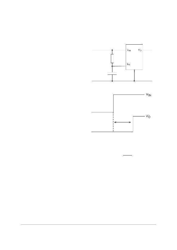
�Start� up� delay�
�A� small� amount� of� hysteresis� is� provided� on� the�
�Enable� pin� to� ensure� clean� switching.� This�
�feature� can� be� used� to� introduce� a� start� up� delay�
�if� required.� Addition� of� a� simple� RC� network� on�
�the� Enable� pin� provides� this� function.� The�
�following� diagram� illustrates� this� circuit�
�connection.� The� equation� provided� enables�
�calculation� of� the� delay� period.�
�R�
�C�
�Figure� 1� Circuit� Connection�
�T� d�
�Figure� 2� Start� up� delay� (T� d� )�
�?� V� IN� ?�
�?� V� IN� ?� 1.5� ?�
�Calculation� of� start� up� delay� as� above�
��?� Zetex� Semiconductors� plc� 2007�
�9�
��相关PDF资料 |
PDF描述 |
|---|---|
| TAJS684K020RNJ | CAP TANT 0.68UF 20V 10% 1206 |
| GBC05DRYN-S734 | CONN EDGECARD 10POS DIP .100 SLD |
| ABM22DTMT-S664 | CONN EDGECARD 44POS R/A .156 |
| 180-M62-213R001 | CONN DB62 FMAL HD SLD DIP NICKEL |
| TAJS684K016RNJ | CAP TANT 0.68UF 16V 10% 1206 |
相关代理商/技术参数 |
参数描述 |
|---|---|
| ZXCM209 | 制造商:ZETEX 制造商全称:ZETEX 功能描述:VERY LOW POWER MICROPROCESSOR RESET DEVICES |
| ZXCM209JF | 制造商:未知厂家 制造商全称:未知厂家 功能描述:Voltage Detector |
| ZXCM209LF | 制造商:未知厂家 制造商全称:未知厂家 功能描述:Voltage Detector |
| ZXCM209LFTA | 制造商:未知厂家 制造商全称:未知厂家 功能描述:IC-SM-SUPERVISORY CIRCUIT |
| ZXCM209MF | 制造商:未知厂家 制造商全称:未知厂家 功能描述:Voltage Detector |
发布紧急采购,3分钟左右您将得到回复。