- 您现在的位置:买卖IC网 > PDF目录24690 > 05F6930 IC-ANALOGUE MULTIPLIER PDF资料下载
参数资料
| 型号: | 05F6930 |
| 英文描述: | IC-ANALOGUE MULTIPLIER |
| 中文描述: | 集成电路模拟乘法器 |
| 文件页数: | 3/12页 |
| 文件大小: | 347K |
| 代理商: | 05F6930 |
AD524C
RG2
RG1
2
16
13
12
11
3
1
+Vs
8
7
–Vs
9
6
10
4
5
G = 100
10k
14-BIT
ADC
0 TO 2V
F.S.
+10V
350
350
350
350
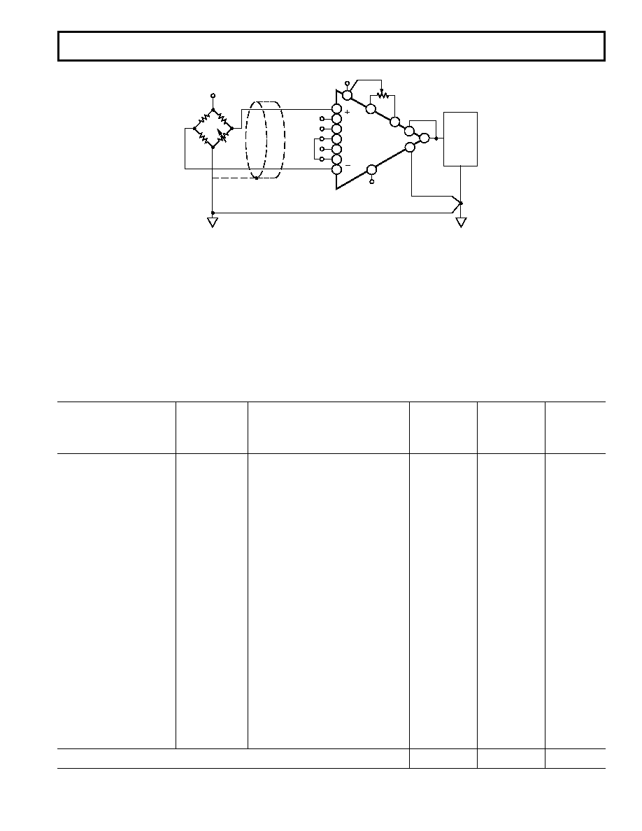
Figure 46. Typical Bridge Application
REV. C
–11–
Error Budget Analysis–AD524
Table II. Error Budget Analysis of AD524CD in Bridge Application
Effect on
Absolute
Effect
AD524C
Accuracy
on
Error Source
Specifications
Calculation
at TA = 25
°C
at TA = 85
°C Resolution
Gain Error
±0.25%
±0.25% = 2500 ppm
2500 ppm
–
Gain Instability
25 ppm
(25 ppm/
°C)(60°C) = 1500 ppm
–
1500 ppm
–
Gain Nonlinearity
±0.003%
±0.003% = 30 ppm
–
30 ppm
Input Offset Voltage
±50 V, RTI
±50 V/20 mV = ±2500 ppm
2500 ppm
–
Input Offset Voltage Drift
±0.5 V/°C(±0.5 V/°C)(60°C) = 30 V
–
30
V/20 mV = 1500 ppm
–
1500 ppm
–
Output Offset Voltage
l
±2.0 mV
±2.0 mV/20 mV = 1000 ppm
1000 ppm
–
Output Offset Voltage Drift
1
±25 V/°C(±25 V/°C)(60°C)= 1500 V
1500
V/20 mV = 750 ppm
–
750 ppm
–
Bias Current-Source
±15 nA
(
±15 nA)(100 ) = 1.5 V
Imbalance Error
1.5
V/20 mV = 75 ppm
75 ppm
–
Bias Current-Source
±100 pA/°C(±100 pA/°C)(100 )(60°C) = 0.6 V
Imbalance Drift
0.6
V/20 mV= 30 ppm
–
30 ppm
–
Offset Current-Source
±10 nA
(
±10 nA)(100 ) = 1 V
Imbalance Error
1
V/20 mV = 50 ppm
50 ppm
–
Offset Current-Source
±100 pA/°C
(100 pA/
°C)(100 )(60°C) = 0.6 V
Imbalance Drift
0.6
V/20 mV = 30 ppm
–
30 ppm
–
Offset Current-Source
±10 nA
(10 nA)(175
) = 3.5 V
Resistance-Error
3.5
V/20 mV = 87.5 ppm
87.5 ppm
–
Offset Current-Source
±100 pA/°C
(100 pA/
°C)(175 )(60°C) = 1 V
Resistance-Drift
1
V/20 mV = 50 ppm
–
50 ppm
–
Common Mode Rejection
115 dB
115 dB = 1.8 ppm
× 5 V = 8.8 V
5 V dc
8.8
V/20 mV = 444 ppm
444 ppm
–
Noise, RTI
(0.1 Hz–10 Hz)
0.3
V p-p
0.3
V p-p/20 mV = 15 ppm
–
15 ppm
Total Error
6656.5 ppm
10516.5 ppm 45 ppm
1Output offset voltage and output offset voltage drift are given as RTI figures.
ERROR BUDGET ANALYSIS
To illustrate how instrumentation amplifier specifications are
applied, we will now examine a typical case where an AD524 is
required to amplify the output of an unbalanced transducer.
Figure 46 shows a differential transducer, unbalanced by 100
,
supplying a 0 to 20 mV signal to an AD524C. The output of the
IA feeds a 14-bit A to D converter with a 0 to 2 volt input volt-
age range. The operating temperature range is –25
°C to +85°C.
Therefore, the largest change in temperature
T within the op-
erating range is from ambient to +85
°C (85°C –25°C = 60°C).
In many applications, differential linearity and resolution are of
prime importance. This would be so in cases where the absolute
value of a variable is less important than changes in value. In
these applications, only the irreducible errors (45ppm =
0.004%) are significant. Furthermore, if a system has an intelli-
gent processor monitoring the A to D output, the addition of a
auto-gain/auto-zero cycle will remove all reducible errors and
may eliminate the requirement for initial calibration. This will
also reduce errors to 0.004%.
相关PDF资料 |
PDF描述 |
|---|---|
| 05F6950 | IC-COMPUTATION CIRCUIT |
| 05F6971 | IC-ELECTROMETER AMPLIFIER |
| 934045690118 | BUF OR INV BASED PRPHL DRVR |
| 934045770114 | S BAND, Si, NPN, RF POWER TRANSISTOR |
| 934045780114 | S BAND, Si, NPN, RF POWER TRANSISTOR |
相关代理商/技术参数 |
参数描述 |
|---|---|
| 05FD101J03 | 制造商: 功能描述: 制造商:undefined 功能描述: |
| 05FD111J03 | 制造商: 功能描述: 制造商:undefined 功能描述: |
| 05FD161J03 | 制造商: 功能描述: 制造商:undefined 功能描述: |
| 05FD241J03 | 制造商: 功能描述: 制造商:undefined 功能描述: |
| 05FD271J03 | 制造商: 功能描述: 制造商:undefined 功能描述: |
发布紧急采购,3分钟左右您将得到回复。