- 您现在的位置:买卖IC网 > PDF目录24690 > 05F6950 IC-COMPUTATION CIRCUIT PDF资料下载
参数资料
| 型号: | 05F6950 |
| 英文描述: | IC-COMPUTATION CIRCUIT |
| 中文描述: | 集成电路计算电路 |
| 文件页数: | 1/12页 |
| 文件大小: | 347K |
| 代理商: | 05F6950 |
REV. C
Information furnished by Analog Devices is believed to be accurate and
reliable. However, no responsibility is assumed by Analog Devices for its
use, nor for any infringements of patents or other rights of third parties
which may result from its use. No license is granted by implication or
otherwise under any patent or patent rights of Analog Devices.
a
Precision
Instrumentation Amplifier
AD524
FEATURES
Low Noise: 0.3
V p-p 0.1 Hz to 10 Hz
Low Nonlinearity: 0.003% (G = 1)
High CMRR: 120 dB (G = 1000)
Low Offset Voltage: 50
V
Low Offset Voltage Drift: 0.5
V/ C
Gain Bandwidth Product: 25 MHz
Pin Programmable Gains of 1, 10, 100,1000
Input Protection, Power On–Power Off
No External Components Required
Internally Compensated
MIL-STD-883B and Chips Available
16-Pin Ceramic DIP and SOIC Packages and
20-Terminal Leadless Chip Carriers Available
Available in Tape and Reel in Accordance
with EIA-481A Standard
Standard Military Drawing Also Available
PRODUCT DESCRIPTION
The AD524 is a precision monolithic instrumentation amplifier
designed for data acquisition applications requiring high accu-
racy under worst-case operating conditions. An outstanding
combination of high linearity, high common mode rejection, low
offset voltage drift, and low noise makes the AD524 suitable for
use in many data acquisition systems.
The AD524 has an output offset voltage drift of less than 25
V/
°C, input offset voltage drift of less than 0.5 V/°C, CMR above
90 dB at unity gain (120 dB at G = 1000) and maximum
nonlinearity of 0.003% at G = 1. In addition to the outstanding
dc specifications the AD524 also has a 25 MHz gain bandwidth
product (G = 100). To make it suitable for high speed data ac-
quisition systems the AD524 has an output slew rate of 5 V/
s
and settles in 15
s to 0.01% for gains of 1 to 100.
As a complete amplifier the AD524 does not require any exter-
nal components for fixed gains of 1, 10, 100 and 1,000. For
other gain settings between 1 and 1000 only a single resistor is
required. The AD524 input is fully protected for both power on
and power off fault conditions.
The AD524 IC instrumentation amplifier is available in four
different versions of accuracy and operating temperature range.
The economical “A” grade, the low drift “B” grade and lower
drift, higher linearity “C” grade are specified from –25
°C to
+85
°C. The “S” grade guarantees performance to specification
over the extended temperature range –55
°C to +125°C. Devices
are available in 16-pin ceramic DIP and SOIC packages and a
20-terminal leadless chip carrier.
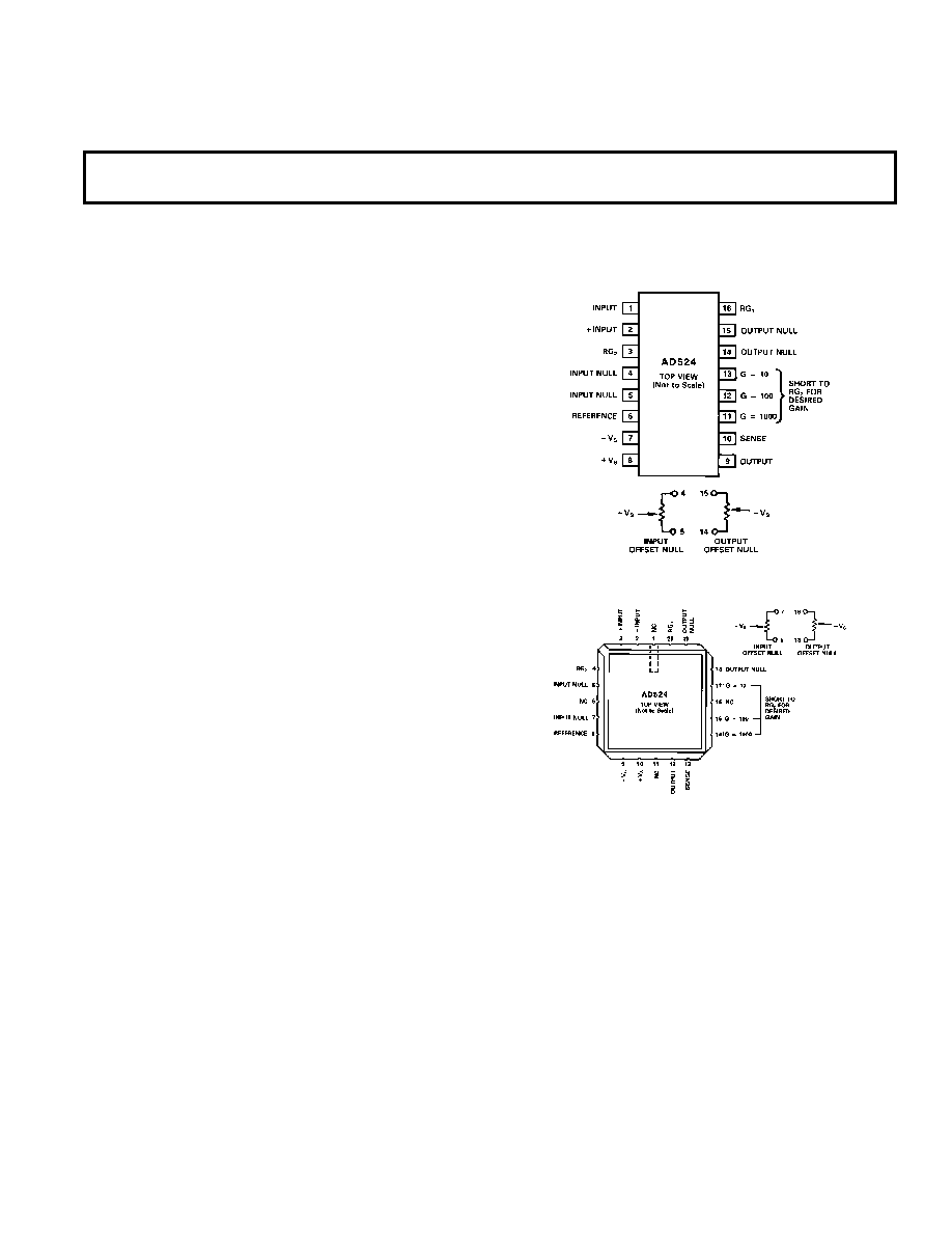
CONNECTION DIAGRAMS
Ceramic (D) and
SOIC (R) Packages
Leadless Chip Carrier (E) Package
PRODUCT HIGHLIGHTS
1. The AD524 has guaranteed low offset voltage, offset voltage
drift and low noise for precision high gain applications.
2. The AD524 is functionally complete with pin programmable
gains of 1, 10, 100 and 1000, and single resistor program-
mable for any gain.
3. Input and output offset nulling terminals are provided for
very high precision applications and to minimize offset volt-
age changes in gain ranging applications.
4. The AD524 is input protected for both power on and power
off fault conditions.
5. The AD524 offers superior dynamic performance with a gain
bandwidth product of 25 MHz, full power response of 75 kHz
and a settling time of 15
s to 0.01% of a 20 V step (G = 100).
One Technology Way, P.O. Box 9106, Norwood, MA 02062-9106, U.S.A.
Tel: 617/329-4700
Fax: 617/326-8703
相关PDF资料 |
PDF描述 |
|---|---|
| 05F6971 | IC-ELECTROMETER AMPLIFIER |
| 934045690118 | BUF OR INV BASED PRPHL DRVR |
| 934045770114 | S BAND, Si, NPN, RF POWER TRANSISTOR |
| 934045780114 | S BAND, Si, NPN, RF POWER TRANSISTOR |
| 934045790114 | S BAND, Si, NPN, RF POWER TRANSISTOR |
相关代理商/技术参数 |
参数描述 |
|---|---|
| 05FD101J03 | 制造商: 功能描述: 制造商:undefined 功能描述: |
| 05FD111J03 | 制造商: 功能描述: 制造商:undefined 功能描述: |
| 05FD161J03 | 制造商: 功能描述: 制造商:undefined 功能描述: |
| 05FD241J03 | 制造商: 功能描述: 制造商:undefined 功能描述: |
| 05FD271J03 | 制造商: 功能描述: 制造商:undefined 功能描述: |
发布紧急采购,3分钟左右您将得到回复。