参数资料
| 型号: | 101-0814 |
| 厂商: | Rabbit Semiconductor |
| 文件页数: | 80/94页 |
| 文件大小: | 0K |
| 描述: | COMPUTER SNG BD BL1810 512K SRAM |
| 标准包装: | 10 |
| 系列: | SBC |
| 模块/板类型: | 单板计算机模块 |
| 适用于相关产品: | BL1810 |
第1页第2页第3页第4页第5页第6页第7页第8页第9页第10页第11页第12页第13页第14页第15页第16页第17页第18页第19页第20页第21页第22页第23页第24页第25页第26页第27页第28页第29页第30页第31页第32页第33页第34页第35页第36页第37页第38页第39页第40页第41页第42页第43页第44页第45页第46页第47页第48页第49页第50页第51页第52页第53页第54页第55页第56页第57页第58页第59页第60页第61页第62页第63页第64页第65页第66页第67页第68页第69页第70页第71页第72页第73页第74页第75页第76页第77页第78页第79页当前第80页第81页第82页第83页第84页第85页第86页第87页第88页第89页第90页第91页第92页第93页第94页
User’s Manual
77
Once the LEDs, resistors, and switches are disconnected as described above, the user has a
Jackrabbit board with connection points conveniently brought out to labeled points at headers
J3 and J7 on the Prototyping Board. Small to medium circuits can be prototyped using point-
to-point wiring with 20 to 30 AWG wire between the prototyping area and the holes at loca-
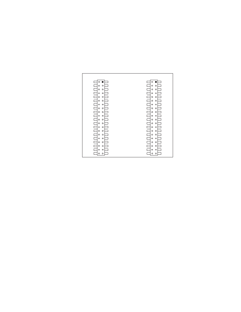
tions J3 and J7. Note that the pinouts at locations J3 and J7 on the top side of the Prototyping
Board (shown in Figure B-7) are a mirror image of the Jackrabbit board pinouts.
Figure B-7. Jackrabbit I/O Pinout on Prototyping Board (top side)
A user-supplied DE9 connector can be added as shown in Figure B-3. The signals are
brought out to location J5 on the top side of the Prototyping Board.
There are six independent surface-mount 14- to 16-pin SOIC pads and fourteen 3- to 5-pin
SOT23 pads. Each component has every one of its pin pads connected to a hole in the pro-
totyping area. The layout is such that there is another SOIC or SOT23 pad directly on the
other side of the PCB from the SOIC or SOT23 pads. However, each layout location is
routed to its unique set of connection holes. Because the traces are very thin, carefully
determine which set of holes is connected to which surface-mount pad. There are several
standard 0805 passive-component surface-mount pads. These pads are not routed to wir-
ing holes so wire must be soldered directly to the component. In addition, there is a large
generic array of wide traces connected to large holes. This is provided as an additional
area for surface-mount passive components. There is a moderate amount of 0.1” arrayed
through-hole prototyping area (about 137 holes) for mounting through-hole components.
Thus, many circuits requiring special circuitry external to the Jackrabbit can be prototyped
and tested with the Prototyping Board. If additional prototyping space is needed, install
40-pin headers at locations J3 and J7 on the top side of the Prototyping Board to connect
to sockets that you would install at J3 and J7 on the top side of a second Prototyping
Board.
J7
VCC
PA1
PA3
PA5
PA7
GND
PB1
PB3
PB5
PB7
PCLK
PE7
PE5
PE3
PE1
GND
HV1
HV3
+RAW
VCC
J3
GND
PA0
PA2
PA4
PA6
GND
PB0
PB2
PB4
PB6
WDO
GND
PE6
PE4
PE2
PE0
HV0
HV2
K
GND
VCC
RXB
TXB
PC0
PC2
PC4
PC6
AD0
DA0
PD0
PD2
PD4
PD6
GND
485
VCC
SM0
IOBEN
GND
/RST
GND
RXC
TXC
PC1
PC3
PC5
PC7
AGND
DA1
PD1
PD3
PD5
PD7
GND
485+
VCC
SM1
STAT
VBAT
GND
相关PDF资料 |
PDF描述 |
|---|---|
| 101-1007 | MODULE POWERCORE FLEX 3810 |
| 101-1028 | MODULE RABBITCORE RCM3750 |
| 101-1087 | MODULE RABBITCORE RCM 3365 |
| 1B31AN | IC SIGNAL COND STRAIN GAGE 28DIP |
| 1B32AN | IC SIGNAL COND HYBRID 28-DIP |
相关代理商/技术参数 |
参数描述 |
|---|---|
| 101-0815 | 功能描述:单板计算机 SR9100 512K SRAM RoHS:否 制造商:Ampro By ADLINK 外观尺寸:EPIC 处理器类型:Intel Atom D510 频率:1.66 GHz 存储容量:2 GB (max) 存储类型:DDR2, L2 Cache 接口类型:Ethernet, PS/2, SATA, Serial, USB 工作电源电压:5 V, 12 V 功耗:13 W 最大工作温度:+ 70 C 尺寸:165.1 mm x 114.3 mm |
| 101-0816 | 功能描述:KIT DEV RABBITCORE TCP/IP 2000 RoHS:否 类别:编程器,开发系统 >> 过时/停产零件编号 系列:* 标准包装:1 系列:- 类型:MCU 适用于相关产品:Freescale MC68HC908LJ/LK(80-QFP ZIF 插口) 所含物品:面板、缆线、软件、数据表和用户手册 其它名称:520-1035 |
| 101-0817 | 功能描述:单板计算机 BL2030 512K SRAM RoHS:否 制造商:Ampro By ADLINK 外观尺寸:EPIC 处理器类型:Intel Atom D510 频率:1.66 GHz 存储容量:2 GB (max) 存储类型:DDR2, L2 Cache 接口类型:Ethernet, PS/2, SATA, Serial, USB 工作电源电压:5 V, 12 V 功耗:13 W 最大工作温度:+ 70 C 尺寸:165.1 mm x 114.3 mm |
| 101-0818 | 功能描述:单板计算机 BL2100 Fric Lk 512K RoHS:否 制造商:Ampro By ADLINK 外观尺寸:EPIC 处理器类型:Intel Atom D510 频率:1.66 GHz 存储容量:2 GB (max) 存储类型:DDR2, L2 Cache 接口类型:Ethernet, PS/2, SATA, Serial, USB 工作电源电压:5 V, 12 V 功耗:13 W 最大工作温度:+ 70 C 尺寸:165.1 mm x 114.3 mm |
| 101-0820 | 功能描述:COMPUTER SGL-BD BL2000 SRAM/FLSH RoHS:否 类别:集成电路 (IC) >> 嵌入式 - 微控制器或微处理器模块 系列:SBC 产品目录绘图:DLP-245SY-G 标准包装:1 系列:USB 模块/板类型:开发板 适用于相关产品:USB 其它名称:813-1006 |
发布紧急采购,3分钟左右您将得到回复。