- 您现在的位置:买卖IC网 > PDF目录293732 > 1245FAFC (TRIQUINT SEMICONDUCTOR INC) TRANSMITTER PDF资料下载
参数资料
| 型号: | 1245FAFC |
| 厂商: | TRIQUINT SEMICONDUCTOR INC |
| 元件分类: | 数字传输电路 |
| 英文描述: | TRANSMITTER |
| 封装: | PLASTIC, DIP-20 |
| 文件页数: | 8/12页 |
| 文件大小: | 201K |
| 代理商: | 1245FAFC |
Lucent Technologies Inc.
5
Data Sheet
September 1999
1241/1243/1245-Type Uncooled Laser Transmitter
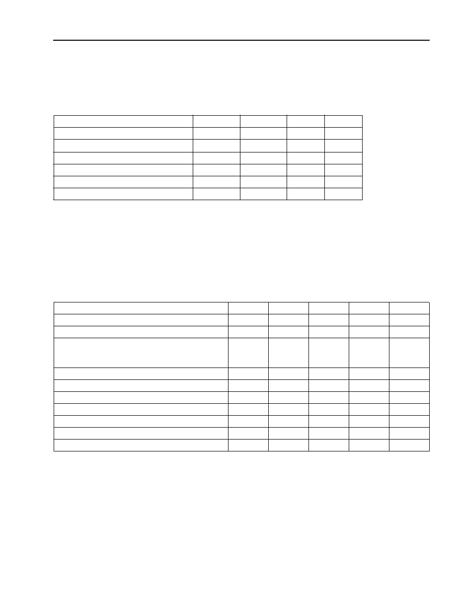
Absolute Maximum Ratings
Stresses in excess of the absolute maximum ratings can cause permanent damage to the device. These are abso-
lute stress ratings only. Functional operation of the device is not implied at these or any other conditions in excess
of those given in the operations sections of the data sheet. Exposure to absolute maximum ratings for extended
periods can adversely affect device reliability.
* With VEE connected to –5 V, VCC must be at 0 V; with VCC connected to +5 V, VEE must be at 0 V.
Specication depends upon the code ordered. The device is capable of a cold start at –40
°C; specications are met
after a warm-up time determined by the system thermal design.
Characteristics
Minimum and maximum values specied over operating case temperature range at 50% duty cycle data signal and
end of life (EOL). Typical values are measured at beginning-of-life (BOL) room temperature unless otherwise noted.
Table 2. Electrical Characteristics
1. With VEE connected to –5 V, VCC must be at 0 V; with VCC connected to +5 V, VEE must be at 0 V.
2. Input measured from VCC with 50
load to (VCC – 2 V). 10K, 10K H, and 100K ECL compatible.
3. Between 10% and 90% (50% duty cycle) where t is the bit period in ns.
4. The transmitter is normally enabled and only requires an external voltage to disable.
5. Time measured from rising edge of disable signal until optical output (laser diode) has turned off.
6. Time measured from falling edge of enable signal until optical output has stabilized at nominal output power level.
7. The laser bias current is obtained by dividing the bias voltage by the 10
current-sensing resistors. (See Figure 1.) When measuring these
voltages or using them in conjunction with alarm circuits, use a high-input impedance device.
8. The laser back-facet monitor voltage is a scaled output that tracks the transmitter optical output power.
Parameter
Symbol
Min
Max
Unit
Supply Voltage*
—
5.5
V
Operating Case Temperature Range
TC
–40
85
°C
Storage Case Temperature Range
Tstg
–40
85
°C
Lead Soldering Temperature/Time
—
250/10
°C/s
Relative Humidity (noncondensing)
RH
—
85
%
Minimum Fiber Bend Radius
—
1.00 (25.4)
—
in. (mm)
Parameter
Symbol
Min
Typ
Max
Unit
Power Supply Voltage1
V
4.75
5.0
5.50
V
Power Supply Current Drain
ITOTAL
—
30
130
mA
Input Data Voltage:2
Low
High
VIL
VIH
–1.81
–1.16
—
–1.47
–0.88
V
Input Transition Time3
tI
—
t/4
—
ns
Transmitter Disable Voltage4
VD
VCC – 2.0
—
VCC
V
Transmitter Enable Voltage
VEN
VEE
—VEE + 0.8
V
Output Disable Time5
tD
—
0.20
s
Output Enable Time6
tEN
—
2.00
s
Laser Bias Voltage7
VB
0.01
0.06
0.70
V
Laser Monitor Voltage (50% duty cycle)8
VBF
0.01
0.05
0.20
V
相关PDF资料 |
PDF描述 |
|---|---|
| 1245CBDC | TRANSMITTER |
| 1245CAFC | TRANSMITTER |
| 1243FBDC | TRANSMITTER |
| 1243FAFD | TRANSMITTER |
| 1243CBDC | TRANSMITTER |
相关代理商/技术参数 |
参数描述 |
|---|---|
| 1245FBDC | 制造商:AGERE 制造商全称:AGERE 功能描述:1241/1243/1245-Type Uncooled Laser Transmitter |
| 1245G0 | 制造商:未知厂家 制造商全称:未知厂家 功能描述:Peripheral IC |
| 1245G1 | 制造商:未知厂家 制造商全称:未知厂家 功能描述:Peripheral IC |
| 1245G2 | 制造商:未知厂家 制造商全称:未知厂家 功能描述:Peripheral IC |
| 1245M0 | 制造商:未知厂家 制造商全称:未知厂家 功能描述:Peripheral IC |
发布紧急采购,3分钟左右您将得到回复。