参数资料
| 型号: | 23A256T-I/SN |
| 厂商: | Microchip Technology |
| 文件页数: | 13/28页 |
| 文件大小: | 0K |
| 描述: | IC SRAM 256KBIT 20MHZ 8SOIC |
| 产品培训模块: | 23x640 and 23x256 SRAM Overview |
| 标准包装: | 3,300 |
| 格式 - 存储器: | RAM |
| 存储器类型: | SRAM |
| 存储容量: | 256K (32K x 8) |
| 速度: | 20MHz |
| 接口: | SPI 串行 |
| 电源电压: | 1.7 V ~ 1.95 V |
| 工作温度: | -40°C ~ 85°C |
| 封装/外壳: | 8-SOIC(0.154",3.90mm 宽) |
| 供应商设备封装: | 8-SOICN |
| 包装: | 带卷 (TR) |
第1页第2页第3页第4页第5页第6页第7页第8页第9页第10页第11页第12页当前第13页第14页第15页第16页第17页第18页第19页第20页第21页第22页第23页第24页第25页第26页第27页第28页
�� �
�
�23A256/23K256�
�3.0�
�PIN� DESCRIPTIONS�
�3.5�
�Hold� (HOLD)�
�The� descriptions� of� the� pins� are� listed� in� Table� 3-1� .�
�The� HOLD� pin� is� used� to� suspend� transmission� to� the�
�23X256� while� in� the� middle� of� a� serial� sequence� without�
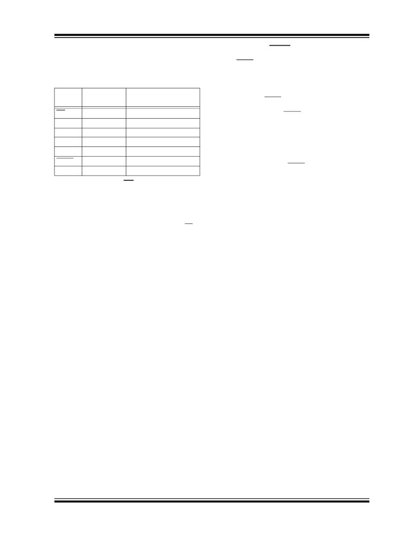
�TABLE� 3-1:�
�PIN� FUNCTION� TABLE�
�having� to� retransmit� the� entire� sequence� again.� It� must�
�be� held� high� any� time� this� function� is� not� being� used.�
�Name�
�CS�
�SO�
�V� SS�
�SI�
�SCK�
�HOLD�
�V� CC�
�PDIP/SOIC�
�TSSOP�
�1�
�2�
�4�
�5�
�6�
�7�
�8�
�Function�
�Chip� Select� Input�
�Serial� Data� Output�
�Ground�
�Serial� Data� Input�
�Serial� Clock� Input�
�Hold� Input�
�Supply� Voltage�
�Once� the� device� is� selected� and� a� serial� sequence� is�
�underway,� the� HOLD� pin� may� be� pulled� low� to� pause�
�further� serial� communication� without� resetting� the�
�serial� sequence.� The� HOLD� pin� must� be� brought� low�
�while� SCK� is� low,� otherwise� the� HOLD� function� will� not�
�be� invoked� until� the� next� SCK� high-to-low� transition.�
�The� 23X256� must� remain� selected� during� this�
�sequence.� The� SI,� SCK� and� SO� pins� are� in� a� high-�
�impedance� state� during� the� time� the� device� is� paused�
�and� transitions� on� these� pins� will� be� ignored.� To� resume�
�serial� communication,� HOLD� must� be� brought� high�
�while� the� SCK� pin� is� low,� otherwise� serial�
�3.1�
�Chip� Select� (CS)�
�communication� will� not� resume.� Lowering� the� HOLD�
�line� at� any� time� will� tri-state� the� SO� line.�
�A� low� level� on� this� pin� selects� the� device.� A� high� level�
�deselects� the� device� and� forces� it� into� Standby� mode.�
�When� the� device� is� deselected,� SO� goes� to� the� high-�
�impedance� state,� allowing� multiple� parts� to� share� the�
�same� SPI� bus.� After� power-up,� a� low� level� on� CS� is�
�required,� prior� to� any� sequence� being� initiated.�
�Hold� functionality� is� disabled� by� the� STATUS� register�
�bit.�
�3.2�
�Serial� Output� (SO)�
�The� SO� pin� is� used� to� transfer� data� out� of� the� 23X256.�
�During� a� read� cycle,� data� is� shifted� out� on� this� pin� after�
�the� falling� edge� of� the� serial� clock.�
�3.3�
�Serial� Input� (SI)�
�The� SI� pin� is� used� to� transfer� data� into� the� device.� It�
�receives� instructions,� addresses� and� data.� Data� is�
�latched� on� the� rising� edge� of� the� serial� clock.�
�3.4�
�Serial� Clock� (SCK)�
�The� SCK� is� used� to� synchronize� the� communication�
�between� a� master� and� the� 23X256.� Instructions,�
�addresses� or� data� present� on� the� SI� pin� are� latched� on�
�the� rising� edge� of� the� clock� input,� while� data� on� the� SO�
�pin� is� updated� after� the� falling� edge� of� the� clock� input.�
�?� 2008-2011� Microchip� Technology� Inc.�
�DS22100F-page� 13�
�相关PDF资料 |
PDF描述 |
|---|---|
| XC2V250-5FG256I | IC FPGA VIRTEX-II 256FGBGA |
| ASM44DRYN-S13 | CONN EDGECARD 88POS .156 EXTEND |
| ASM43DRYI-S13 | CONN EDGECARD 86POS .156 EXTEND |
| ASM44DRYH-S13 | CONN EDGECARD 88POS .156 EXTEND |
| RMC13DTEF | CONN EDGECARD 26POS .100 EYELET |
相关代理商/技术参数 |
参数描述 |
|---|---|
| 23A283F060DD1H1 | 制造商:REGAL BELOIT 功能描述:Electrolytic |
| 23A283F075CG1H1 | 制造商:REGAL BELOIT 功能描述:Electrolytic |
| 23A283F080DF1H1 | 制造商:REGAL BELOIT 功能描述:Electrolytic |
| 23A-30 | 制造商:Aeroflex / Inmet 功能描述:ATTENUATOR - FIXED COAXIAL |
| 23A323F050BI1H1 | 制造商:REGAL BELOIT 功能描述:Electrolytic |
发布紧急采购,3分钟左右您将得到回复。