- 您现在的位置:买卖IC网 > PDF目录4556 > 24LC01BT-I/MNY (Microchip Technology)IC EEPROM 1KBIT 400KHZ 8TDFN PDF资料下载
参数资料
| 型号: | 24LC01BT-I/MNY |
| 厂商: | Microchip Technology |
| 文件页数: | 6/34页 |
| 文件大小: | 0K |
| 描述: | IC EEPROM 1KBIT 400KHZ 8TDFN |
| 标准包装: | 1 |
| 格式 - 存储器: | EEPROMs - 串行 |
| 存储器类型: | EEPROM |
| 存储容量: | 1K (128 x 8) |
| 速度: | 400kHz |
| 接口: | I²C,2 线串口 |
| 电源电压: | 2.5 V ~ 5.5 V |
| 工作温度: | -40°C ~ 85°C |
| 封装/外壳: | 8-WFDFN 裸露焊盘 |
| 供应商设备封装: | 8-TDFN(2x3) |
| 包装: | 标准包装 |
| 产品目录页面: | 1444 (CN2011-ZH PDF) |
| 其它名称: | 24LC01BT-I/MNYDKR |
第1页第2页第3页第4页第5页当前第6页第7页第8页第9页第10页第11页第12页第13页第14页第15页第16页第17页第18页第19页第20页第21页第22页第23页第24页第25页第26页第27页第28页第29页第30页第31页第32页第33页第34页
�� �
�
�24AA01/24LC01B�
�3.0�
�FUNCTIONAL� DESCRIPTION�
�4.4�
�Data� Valid� (D)�
�The� 24XX01� supports� a� bidirectional,� 2-wire� bus� and�
�data� transmission� protocol.� A� device� that� sends� data�
�onto� the� bus� is� defined� as� transmitter,� while� defining� a�
�device� receiving� data� as� a� receiver.� The� bus� has� to� be�
�controlled� by� a� master� device� which� generates� the�
�Serial� Clock� (SCL),� controls� the� bus� access� and�
�generates� the� Start� and� Stop� conditions,� while� the�
�24XX01� works� as� slave.� Both� master� and� slave� can�
�operate� as� transmitter� or� receiver,� but� the� master�
�device� determines� which� mode� is� activated.�
�The� state� of� the� data� line� represents� valid� data� when,�
�after� a� Start� condition,� the� data� line� is� stable� for� the�
�duration� of� the� high� period� of� the� clock� signal.�
�The� data� on� the� line� must� be� changed� during� the� low�
�period� of� the� clock� signal.� There� is� one� clock� pulse� per�
�bit� of� data.�
�Each� data� transfer� is� initiated� with� a� Start� condition� and�
�terminated� with� a� Stop� condition.� The� number� of� data�
�bytes� transferred� between� the� Start� and� Stop�
�conditions� is� determined� by� the� master� device� and� is,�
�4.0�
�BUS� CHARACTERISTICS�
�theoretically,� unlimited� (although� only� the� last� sixteen�
�will� be� stored� when� doing� a� write� operation).� When� an�
�The� following� bus� protocol� has� been� defined:�
�?� Data� transfer� may� be� initiated� only� when� the� bus�
�overwrite� does� occur,� it� will� replace� data� in� a� first-in�
�first-out� (FIFO)� fashion.�
�is� not� busy.�
�?� During� data� transfer,� the� data� line� must� remain�
�4.5�
�Acknowledge�
�stable� whenever� the� clock� line� is� high.� Changes� in�
�the� data� line� while� the� clock� line� is� high� will� be�
�interpreted� as� a� Start� or� Stop� condition.�
�Accordingly,� the� following� bus� conditions� have� been�
�Each� receiving� device,� when� addressed,� is� obliged� to�
�generate� an� acknowledge� after� the� reception� of� each�
�byte.� The� master� device� must� generate� an� extra� clock�
�pulse� which� is� associated� with� this� Acknowledge� bit.�
�defined� (Figure� 4-1).�
�Note:�
�The� 24XX01� does� not� generate� any�
�Acknowledge� bits� if� an� internal�
�4.1�
�Bus� Not� Busy� (A)�
�programming� cycle� is� in� progress.�
�Both� data� and� clock� lines� remain� high.�
�The� device� that� acknowledges� has� to� pull� down� the�
�SDA� line� during� the� acknowledge� clock� pulse� in� such� a�
�4.2�
�Start� Data� Transfer� (B)�
�way� that� the� SDA� line� is� stable-low� during� the� high�
�period� of� the� acknowledge-related� clock� pulse.� Of�
�A� high-to-low� transition� of� the� SDA� line� while� the� clock�
�(SCL)� is� high� determines� a� Start� condition.� All�
�commands� must� be� preceded� by� a� Start� condition.�
�course,� setup� and� hold� times� must� be� taken� into�
�account.� During� reads,� a� master� must� signal� an� end� of�
�data� to� the� slave� by� not� generating� an� Acknowledge� bit�
�on� the� last� byte� that� has� been� clocked� out� of� the� slave.�
�4.3�
�Stop� Data� Transfer� (C)�
�In� this� case,� the� slave� (24XX01)� will� leave� the� data� line�
�high� to� enable� the� master� to� generate� the� Stop�
�A� low-to-high� transition� of� the� SDA� line� while� the� clock�
�(SCL)� is� high� determines� a� Stop� condition.� All�
�operations� must� be� ended� with� a� Stop� condition.�
�condition.�
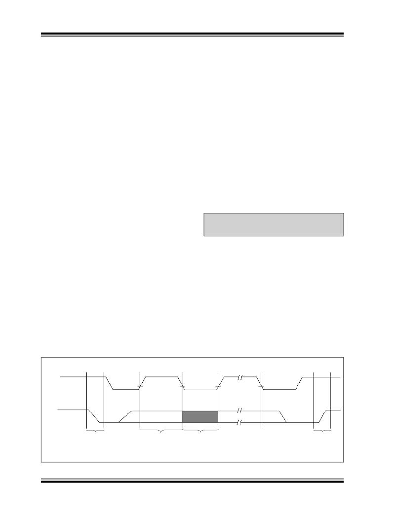
�FIGURE� 4-1:�
�DATA� TRANSFER� SEQUENCE� ON� THE� SERIAL� BUS�
�(A)�
�(B)�
�(D)�
�(D)�
�(C)�
�(A)�
�SCL�
�SDA�
�Start�
�Condition�
�Address� or�
�Acknowledge�
�Data�
�Allowed�
�Stop�
�Condition�
�DS21711J-page� 6�
�Valid�
�to� Change�
�?� 2009� Microchip� Technology� Inc.�
�相关PDF资料 |
PDF描述 |
|---|---|
| RMM36DTMN-S273 | CONN EDGECARD 72POS R/A .156 SLD |
| RMM36DTMD-S273 | CONN EDGECARD 72POS R/A .156 SLD |
| RSM36DTMD-S273 | CONN EDGECARD 72POS R/A .156 SLD |
| 93AA46C-I/SN | IC EEPROM 1KBIT 3MHZ 8SOIC |
| 93LC56B-I/SN | IC EEPROM 2KBIT 3MHZ 8SOIC |
相关代理商/技术参数 |
参数描述 |
|---|---|
| 24LC01BTISN | 制造商:MICRO CHIP 功能描述:Pb Free |
| 24LC01BTSN | 制造商:MICROCHIP 功能描述:New |
| 24LC01-E/MSG | 制造商:MICROCHIP 制造商全称:Microchip Technology 功能描述:1K I2C Serial EEPROM |
| 24LC01-E/OTG | 制造商:MICROCHIP 制造商全称:Microchip Technology 功能描述:1K I2C Serial EEPROM |
| 24LC01-E/PG | 制造商:MICROCHIP 制造商全称:Microchip Technology 功能描述:1K I2C Serial EEPROM |
发布紧急采购,3分钟左右您将得到回复。