- 您现在的位置:买卖IC网 > PDF目录33224 > 2N2920DCSMG4 (SEMELAB LTD) 50 mA, 60 V, 2 CHANNEL, NPN, Si, SMALL SIGNAL TRANSISTOR PDF资料下载
参数资料
| 型号: | 2N2920DCSMG4 |
| 厂商: | SEMELAB LTD |
| 元件分类: | 小信号晶体管 |
| 英文描述: | 50 mA, 60 V, 2 CHANNEL, NPN, Si, SMALL SIGNAL TRANSISTOR |
| 封装: | HERMETIC SEALED, CERAMIC, LCC2-6 |
| 文件页数: | 2/4页 |
| 文件大小: | 26K |
| 代理商: | 2N2920DCSMG4 |
2N2920DCSM
Semelab plc. Telephone (01455) 556565. Telex: 341927. Fax (01455) 552612.
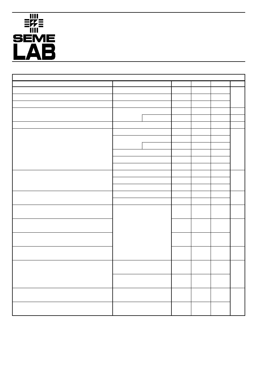
Parameter
Test Conditions 1
Min.
Typ.
Max.
Unit
V
nA
A
nA
—
V
k
—
mho
—
pF
60
5
10
20
100
150
450
75
150
450
300
125
–0.7
–0.8
–0.2
–0.25
330
150
600
25 x 10-4
560
1
15
4
8
V(BR)CBO
Collector – Base Breakdown Voltage
V(BR)CEO* Collector – Emitter Breakdown Voltage
V(BR)EBO
Emitter – Base Breakdown Voltage
ICBO
Collector Cut-off Current
IEBO
Emitter Cut-off Current
hFE
DC Current Gain
VBE
Base – Emitter Voltage
VCE(sat)
Collector – Emitter Saturation Voltage
hie
Small Signal Common – Emitter
Input Impedance
hfe
Small Signal Common – Emitter
Current Gain
hre
Small Signal Common – Emitter
Reverse Voltage Gain
hoe
Small Signal Common – Emitter
Output Admittance
|hfe|
Small Signal Common – Emitter
Current Gain
Cobo
Common – Base Open Circuit
Output Capacitance
Cibo
Common – Base Open Circuit
Input Capacitance
IC = –10AIE = 0
IC = –10mA
IB = 0
IE = –10AIC = 0
VCB = –50V
IE = 0
TA = 150°C
VEB = –4V
IC = 0
IC = 10AVCE = 5V
IC = –100AVCE = 5V
TA = –55°C
IC = –500AVCE = –5V
IC = –1mA
VCE = –5V
IC = –10mA
VCE = –5V *
IC = –100AVCE = –5V
IB = –10AIC = –100A
IB = –100AIC = –1mA
IB = –10AIC = –100A
IB = –100AIC = –1mA
VCE = –10V
IC = –1mA
f = 1kHz
VCE = –5V
IC = –500A
f = 30MHz
VCE = –5V
IC = –1mA
f = 100MHz
VCB = –5V
IE = 0
f = 100kHz
VEB = –0.5V
IC = 0
f = 100kHz
ELECTRICAL CHARACTERISTICS (Tamb = 25°C unless otherwise stated)
NOTES
* Pulse Test: tp = 300s, δ≤ 2%.
1) Terminals not under test are open circuited under all test conditions.
INDIVIDUAL TRANSISTOR CHARACTERISTICS
Document Number 3735
Issue 1
Semelab Plc reserves the right to change test conditions, parameter limits and package dimensions without notice. Information furnished by Semelab is believed
to be both accurate and reliable at the time of going to press. However Semelab assumes no responsibility for any errors or omissions discovered in its use.
Semelab encourages customers to verify that datasheets are current before placing orders.
相关PDF资料 |
PDF描述 |
|---|---|
| 2N2920LEADFREE | 30 mA, 60 V, 2 CHANNEL, NPN, Si, SMALL SIGNAL TRANSISTOR, TO-78 |
| 2N2920 | 30 mA, 60 V, 2 CHANNEL, NPN, Si, SMALL SIGNAL TRANSISTOR, TO-99 |
| 2N2923 | 100 mA, 25 V, NPN, Si, SMALL SIGNAL TRANSISTOR, TO-92 |
| 2N2926 | 100 mA, 18 V, NPN, Si, SMALL SIGNAL TRANSISTOR, TO-92 |
| 2N3859 | 100 mA, 30 V, NPN, Si, SMALL SIGNAL TRANSISTOR, TO-92 |
相关代理商/技术参数 |
参数描述 |
|---|---|
| 2N2920DCSM-QR-B | 制造商:未知厂家 制造商全称:未知厂家 功能描述:BJT |
| 2N2920JANTX | 制造商:Microsemi Corporation 功能描述: |
| 2N2920JANTXV | 制造商:Microsemi Corporation 功能描述: |
| 2N2920L | 制造商:Microsemi Corporation 功能描述:TRANS GP BJT NPN 60V 0.03A 3PIN TO-78 - Bulk |
| 2N2920U | 制造商:Microsemi Corporation 功能描述:Trans GP BJT NPN 60V 0.03A Case U 制造商:Microsemi Corporation 功能描述:NPN DUAL TRANSISTORS U LAW - Bulk |
发布紧急采购,3分钟左右您将得到回复。