- 您现在的位置:买卖IC网 > PDF目录222234 > 2N4119 (CALOGIC LLC) N-Channel JFET General Purpose Amplifier PDF资料下载
参数资料
| 型号: | 2N4119 |
| 厂商: | CALOGIC LLC |
| 元件分类: | 小信号晶体管 |
| 英文描述: | N-Channel JFET General Purpose Amplifier |
| 中文描述: | N-CHANNEL, Si, SMALL SIGNAL, JFET, TO-72 |
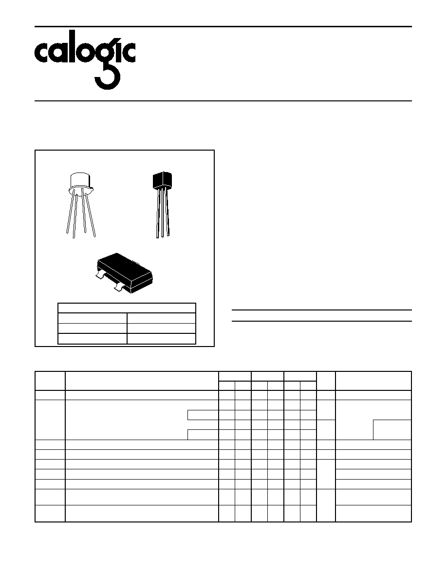
| 封装: | HERMETIC SEALED PACKAGE-4 |
| 文件页数: | 1/1页 |
| 文件大小: | 27K |
| 代理商: | 2N4119 |
N-Channel JFET
General Purpose Amplifier
2N4117 – 2N4119 / 2N4117A – 2N4119A
PN4117 – PN4119 / PN4117A – PN4119A / SST4117 – SST4119
FEATURES
Low Leakage
Low Capacitance
ABSOLUTE MAXIMUM RATINGS
(TA = 25
oC unless otherwise noted)
Gate-Source or Gate-Drain Voltage . . . . . . . . . . . . . . . . -40V
Gate Current . . . . . . . . . . . . . . . . . . . . . . . . . . . . . . . . . 50mA
Storage Temperature Range . . . . . . . . . . . . . -65
oC to +200oC
Operating Temperature Range . . . . . . . . . . . -55
oC to +175oC
Lead Temperature (Soldering, 10sec) . . . . . . . . . . . . . +300
oC
Power Dissipation . . . . . . . . . . . . . . . . . . . . . . . . . . . . 300mW
Derate above 25
oC . . . . . . . . . . . . . . . . . . . . . . . 2.0mW/oC
NOTE: Stresses above those listed under "Absolute Maximum
Ratings" may cause permanent damage to the device. These are
stress ratings only and functional operation of the device at these or
any other conditions above those indicated in the operational sections
of the specifications is not implied. Exposure to absolute maximum
rating conditions for extended periods may affect device reliability.
ORDERING INFORMATION
Part
Package
Temperature Range
2N4117-19/A Hermetic TO-72
-55
oC to +175oC
PN4117-19/A Plastic TO-92
-55
oC to +135oC
SST4117-19
Plastic SOT-23
-55
oC to +135oC
X2N4117-19/A Sorted Chips in Carriers
-55
oC to +175oC
LLC
PIN CONFIGURATION
TO-72
G
D
C
S
ELECTRICAL CHARACTERISTICS (TA = 25
oC unless otherwise specified)
SYMBOL
PARAMETER
4117/A
4118/A
4119/A
UNITS
TEST CONDITIONS
MIN MAX MIN MAX MIN MAX
BVGSS
Gate-Source Breakdown Voltage
-40
V
IG = -1
A, VDS = 0
IGSS
Gate Reverse Current
-10
pA
A devices
-1
VGS = -20V, VDS = 0
-25
nA
TA = +150
oC
A devices
-2.5
VGS(off)
Gate-Source Pinch-Off Voltage
-0.6
-1.8
-1
-3
-2
-6
V
VDS = 10V, ID = 1nA
IDSS
Drain Current at Zero Gate Voltage (Note 1)
0.02 0.09 0.08 0.24 0.20 0.60
mA
VDS = 10V, VGS = 0
gfs
Common-Source Forward Transconductance (Note 1)
7021080250
100
330
S
VDS = 10V, f = 1kHz
gfs
Common-Source Forward Transconductance (Note 2)
60
70
90
VGS = 0, f = 30MHz
gos
Common-Source Output Conductance
35
10
VDS = 10V, VGS = 0, f = 1kHz
Ciss
Common-Source Input Capacitance (Note 2)
333
pF
VDS = 10V, VGS = 0,
f = 1MHz
Crss
Common-Source Reverse Transfer Capacitance (Note 2)
1.5
VDS = 10V, VGS = 0,
f = 1MHz
NOTES: 1. Pulse test: Pulse duration of 2ms used during test.
2. For design reference only, not 100% tested.
D S
G
TO - 92
SOT-23
G
S
D
PRODUCT MARKING (SOT-23)
SST4117
T17
SST4118
T18
SST4119
T19
5007
CALOGIC LLC, 237 WHITNEY PLACE, FREMONT, CA 94539 510-656-2900 PHONE, 510-651-1076 FAX
DS0003 REV A
相关PDF资料 |
PDF描述 |
|---|---|
| 2N4338-41 | N-Channel JFET Low Noise Amplifier |
| 2N4338 | N-Channel JFET Low Noise Amplifier |
| 2N4339 | N-Channel JFET Low Noise Amplifier |
| 2N4340 | N-Channel JFET Low Noise Amplifier |
| 2N4341 | N-Channel JFET Low Noise Amplifier |
相关代理商/技术参数 |
参数描述 |
|---|---|
| 2N4119_TO-71 | 制造商:MICROSS 制造商全称:MICROSS 功能描述:an Ultra-High Input Impedance N-Channel JFET |
| 2N4119A | 功能描述:JFET 40V 0.2mA RoHS:否 制造商:ON Semiconductor 晶体管极性:N-Channel 漏极电流(Vgs=0 时的 Idss):50 mA 漏源电压 VDS:15 V 闸/源击穿电压: 漏极连续电流:50 mA 配置: 安装风格: 封装 / 箱体:SC-59 封装:Reel |
| 2N4119A_TO-71 | 制造商:MICROSS 制造商全称:MICROSS 功能描述:an Ultra-High Input Impedance N-Channel JFET |
| 2N4119A-2 | 制造商:Vishay Siliconix 功能描述:SS SOT23 GP XSTR NPN 65V - Bulk |
| 2N4119A-E3 | 功能描述:JFET 40V 0.2mA RoHS:否 制造商:ON Semiconductor 晶体管极性:N-Channel 漏极电流(Vgs=0 时的 Idss):50 mA 漏源电压 VDS:15 V 闸/源击穿电压: 漏极连续电流:50 mA 配置: 安装风格: 封装 / 箱体:SC-59 封装:Reel |
发布紧急采购,3分钟左右您将得到回复。