- 您现在的位置:买卖IC网 > PDF目录33272 > 2N5566-E3 (VISHAY SILICONIX) 2 CHANNEL, N-CHANNEL, Si, SMALL SIGNAL, JFET, TO-71 PDF资料下载
参数资料
| 型号: | 2N5566-E3 |
| 厂商: | VISHAY SILICONIX |
| 元件分类: | 小信号晶体管 |
| 英文描述: | 2 CHANNEL, N-CHANNEL, Si, SMALL SIGNAL, JFET, TO-71 |
| 封装: | LEAD FREE, HERMETIC SEALED PACKAGE-6 |
| 文件页数: | 1/6页 |
| 文件大小: | 106K |
| 代理商: | 2N5566-E3 |
2N5564/5565/5566
Vishay Siliconix
Document Number: 70254
S-50150—Rev. E, 24-Jan-05
www.vishay.com
1
Matched N-Channel JFET Pairs
PRODUCT SUMMARY
Part Number
VGS(off) (V) V(BR)GSS Min (V) gfs Min (mS) IG Typ (pA) jVGS1 VGS2j Max (mV)
2N5564
0.5 to 3
40
7.5
3
5
2N5565
0.5 to 3
40
7.5
3
10
2N5566
0.5 to 3
40
7.5
3
20
FEATURES
BENEFITS
APPLICATIONS
D Two-Chip Design
D High Slew Rate
D Low Offset/Drift Voltage
D Low Gate Leakage: 3 pA
D Low Noise: 12 nV√Hz @ 10 Hz
D Good CMRR: 76 dB
D Minimum Parasitics
D Tight Differential Match vs. Current
D Improved Op Amp Speed, Settling Time
Accuracy
D Minimum Input Error/Trimming Requirement
D Insignificant Signal Loss/Error Voltage
D High System Sensitivity
D Minimum Error with Large Input Signals
D Maximum High Frequency Performance
D Wideband Differential Amps
D High-Speed,
Temp-Compensated,
Single-Ended Input Amps
D High-Speed Comparators
D Impedance Converters
D Matched Switches
DESCRIPTION
The 2N5564/5565/5566 are matched pairs of JFETs mounted
in a TO-71 package. This two-chip design reduces parasitics
for good performance at high frequency while ensuring
extremely tight matching.
This series features high
breakdown voltage (V(BR)DSS typically > 55 V), high gain
(typically > 9 mS), and <5 mV offset between the two die.
The hermetically-sealed TO-71 package is available with full
military processing (see Military Information).
For similar products see the low-noise U/SST401 series, and
the low-leakage 2N5196/5197/5198/5199 data sheets.
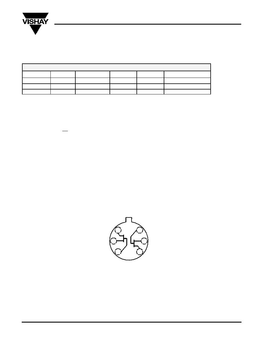
TO-71
Top View
G1
S1
D1
G2
D2
S2
1
2
3
6
5
4
ABSOLUTE MAXIMUM RATINGS
Gate-Drain, Gate-Source Voltage
40 V
. . . . . . . . . . . . . . . . . . . . . . . . . . . . . . .
Gate-Gate Voltage
"80 V
. . . . . . . . . . . . . . . . . . . . . . . . . . . . . . . . . . . . . . . . . . . .
Gate Current
50 mA
. . . . . . . . . . . . . . . . . . . . . . . . . . . . . . . . . . . . . . . . . . . . . . . . .
Lead Temperature (1/16” from case for 10 sec.)
300 _C
. . . . . . . . . . . . . . . . . .
Storage Temperature
65 to 200_C
. . . . . . . . . . . . . . . . . . . . . . . . . . . . . . . . . . .
Operating Junction Temperature
55 to 150_C
. . . . . . . . . . . . . . . . . . . . . . . . . .
Power Dissipation :
Per Sidea
325 mW
. . . . . . . . . . . . . . . . . . . . . . . .
Totalb
650 mW
. . . . . . . . . . . . . . . . . . . . . . . . . . .
Notes
a.
Derate 2.6 mW/_C above 25_C
b.
Derate 5.2 mW/_C above 25_C
相关PDF资料 |
PDF描述 |
|---|---|
| 2N5565-E3 | 2 CHANNEL, N-CHANNEL, Si, SMALL SIGNAL, JFET, TO-71 |
| 2N5566 | N-CHANNEL, Si, SMALL SIGNAL, JFET, TO-71 |
| 2N5564 | N-CHANNEL, Si, SMALL SIGNAL, JFET, TO-71 |
| 2N3972 | N-CHANNEL, Si, SMALL SIGNAL, JFET, TO-18 |
| 2N5575.MOD | 80 A, 70 V, NPN, Si, POWER TRANSISTOR, TO-204AA |
相关代理商/技术参数 |
参数描述 |
|---|---|
| 2N5567 | 制造商:NJSEMI 制造商全称:New Jersey Semi-Conductor Products, Inc. 功能描述:TRIACS BIDIRECTIONAL TRIODE THYRISTORS |
| 2N5568 | 制造商:MOTOROLA 制造商全称:Motorola, Inc 功能描述:BIDIRECTIONAL TRIODE THYRISTORS |
| 2N5569 | 制造商:MOTOROLA 制造商全称:Motorola, Inc 功能描述:BIDIRECTIONAL TRIODE THYRISTORS |
| 2N5570 | 制造商:Fairchild Semiconductor Corporation 功能描述: |
| 2N5571 | 制造商:MOTOROLA 制造商全称:Motorola, Inc 功能描述:SILICON BIDIRECTIOANAL TRIODE THYRISTORS |
发布紧急采购,3分钟左右您将得到回复。