- 您现在的位置:买卖IC网 > PDF目录33272 > 2N5566-E3 (VISHAY SILICONIX) 2 CHANNEL, N-CHANNEL, Si, SMALL SIGNAL, JFET, TO-71 PDF资料下载
参数资料
| 型号: | 2N5566-E3 |
| 厂商: | VISHAY SILICONIX |
| 元件分类: | 小信号晶体管 |
| 英文描述: | 2 CHANNEL, N-CHANNEL, Si, SMALL SIGNAL, JFET, TO-71 |
| 封装: | LEAD FREE, HERMETIC SEALED PACKAGE-6 |
| 文件页数: | 2/6页 |
| 文件大小: | 106K |
| 代理商: | 2N5566-E3 |
2N5564/5565/5566
Vishay Siliconix
www.vishay.com
2
Document Number: 70254
S-50150—Rev. E, 24-Jan-05
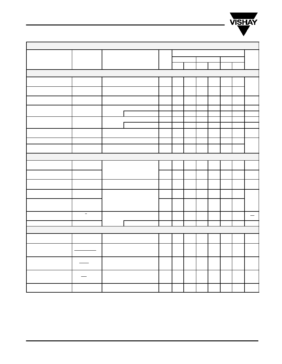
SPECIFICATIONS (TA = 25_C UNLESS OTHERWISE NOTED)
Limits
2N5564
2N5565
2N5566
Parameter
Symbol
Test Conditions
Typa Min Max Min Max Min Max
Unit
Static
Gate-Source
Breakdown Voltage
V(BR)GSS
IG = 1 mA, VDS = 0 V
55
40
V
Gate-Source
Cutoff Voltage
VGS(off)
VDS = 15 V, ID = 1 nA
2
0.5
3
0.5
3
0.5
3
V
Saturation Drain
Currentb
IDSS
VDS = 15 V, VGS = 0 V
20
5
30
5
30
5
30
mA
Gate Reverse Current
IGSS
VGS = 20 V, VDS = 0 V
5
100
pA
Gate Reverse Current
IGSS
TA = 150_C
10
200
nA
Gate Operating Currentc
IG
VDG = 15 V, ID = 2 mA
3
pA
Gate Operating Currentc
IG
TA = 125_C
1
nA
Drain-Source
On-Resistance
rDS(on)
VGS = 0 V, ID = 1 mA
50
100
W
Gate-Source Voltagec
VGS
VDG = 15 V, ID = 2 mA
1.2
Gate-Source
Forward Voltage
VGS(F)
IG = 2 mA , VDS = 0 V
0.7
1
V
Dynamic
Common-Source
Forward Transconductance
gfs
VDS = 15 V, ID = 2 mA
9
7.5
12.5
7.5
12.5
7.5
12.5
mS
Common-Source
Output Conductance
gos
VDS = 15 V, ID = 2 mA
f = 1 kHz
35
45
mS
Common-Source
Forward Transconductanced
gfs
VDS = 15 V, ID = 2 mA
f = 100 MHz
8.5
7
mS
Common-Source
Input Capacitance
Ciss
VDS = 15 V ID = 2 mA
10
12
Common-Source
Reverse Transfer
Capacitance
Crss
VDS = 15 V, ID = 2 mA
f = 1 MHz
2.5
3
pF
Equivalent Input
Noise Voltage
en
VDS = 15 V, ID = 2 mA
f = 10 Hz
12
50
nV
√Hz
Noise Figure
NF
RG = 10 MW
1
dB
Matching
Differential
Gate-Source Voltage
|VGS1–VGS2|
VDG = 15 V, ID = 2 mA
5
10
20
mV
Gate-Source Voltage
Differential Change
with Temperature
D|VGS1–VGS2|
DT
VDG = 15 V, ID = 2 mA
TA = 55 to 125_C
10
25
50
mV/
_C
Saturation Drain
Current Ratioc
IDSS1
IDSS2
VDS = 15 V, VGS = 0 V
0.98
0.95
1
0.95
1
0.95
1
Transconductance Ratio
gfs1
gfs2
VDS = 15 V, ID = 2 mA
f = 1 kHz
0.98
0.95
1
0.90
1
0.90
1
Common Mode
Rejection Ratioc
CMRR
VDG = 10 to 20 V
ID = 2 mA
76
dB
Notes
a.
Typical values are for DESIGN AID ONLY, not guaranteed nor subject to production testing.
NCBD
b.
Pulse test: PW v300 ms duty cycle v3%.
c.
This parameter not registered with JEDEC.
d.
Not a production test.
Stresses beyond those listed under “Absolute Maximum Ratings” may cause permanent damage to the device. These are stress ratings only, and functional operation
of the device at these or any other conditions beyond those indicated in the operational sections of the specifications is not implied. Exposure to absolute maximum
rating conditions for extended periods may affect device reliability.
相关PDF资料 |
PDF描述 |
|---|---|
| 2N5565-E3 | 2 CHANNEL, N-CHANNEL, Si, SMALL SIGNAL, JFET, TO-71 |
| 2N5566 | N-CHANNEL, Si, SMALL SIGNAL, JFET, TO-71 |
| 2N5564 | N-CHANNEL, Si, SMALL SIGNAL, JFET, TO-71 |
| 2N3972 | N-CHANNEL, Si, SMALL SIGNAL, JFET, TO-18 |
| 2N5575.MOD | 80 A, 70 V, NPN, Si, POWER TRANSISTOR, TO-204AA |
相关代理商/技术参数 |
参数描述 |
|---|---|
| 2N5567 | 制造商:NJSEMI 制造商全称:New Jersey Semi-Conductor Products, Inc. 功能描述:TRIACS BIDIRECTIONAL TRIODE THYRISTORS |
| 2N5568 | 制造商:MOTOROLA 制造商全称:Motorola, Inc 功能描述:BIDIRECTIONAL TRIODE THYRISTORS |
| 2N5569 | 制造商:MOTOROLA 制造商全称:Motorola, Inc 功能描述:BIDIRECTIONAL TRIODE THYRISTORS |
| 2N5570 | 制造商:Fairchild Semiconductor Corporation 功能描述: |
| 2N5571 | 制造商:MOTOROLA 制造商全称:Motorola, Inc 功能描述:SILICON BIDIRECTIOANAL TRIODE THYRISTORS |
发布紧急采购,3分钟左右您将得到回复。