- 您现在的位置:买卖IC网 > PDF目录49877 > 2N6515G (ON SEMICONDUCTOR) 500 mA, 250 V, NPN, Si, SMALL SIGNAL TRANSISTOR, TO-92 PDF资料下载
参数资料
| 型号: | 2N6515G |
| 厂商: | ON SEMICONDUCTOR |
| 元件分类: | 小信号晶体管 |
| 英文描述: | 500 mA, 250 V, NPN, Si, SMALL SIGNAL TRANSISTOR, TO-92 |
| 封装: | CASE 29-11, 3 PIN |
| 文件页数: | 1/7页 |
| 文件大小: | 238K |
| 代理商: | 2N6515G |
Semiconductor Components Industries, LLC, 2004
May, 2004 Rev. 4
121
Publication Order Number:
2N6515/D
2N6515, 2N6517, 2N6520
High Voltage Transistors
NPN and PNP
Features
Voltage and Current are Negative for PNP Transistors
PbFree Package is Available*
MAXIMUM RATINGS
Rating
Symbol 2N6515
2N6517
2N6520
Unit
Collector Emitter Voltage
VCEO
250
350
Vdc
Collector Base Voltage
VCBO
250
350
Vdc
Emitter Base Voltage
2N6515, 2N6516, 2N6517
2N6519, 2N6520
VEBO
6.0
5.0
Vdc
Base Current
IB
250
mAdc
Collector Current Continuous
IC
500
mAdc
Total Device Dissipation
@ TA = 25°C
Derate above 25°C
PD
625
5.0
mW
mW/°C
Total Device Dissipation
@ TC = 25°C
Derate above 25°C
PD
1.5
12
Watts
mW/°C
Operating and Storage Junction
Temperature Range
TJ, Tstg
55 to +150
°C
Maximum ratings are those values beyond which device damage can occur.
Maximum ratings applied to the device are individual stress limit values (not nor-
mal operating conditions) and are not valid simultaneously. If these limits are ex-
ceeded, device functional operation is not implied, damage may occur and reli-
ability may be affected.
THERMAL CHARACTERISTICS
Characteristic
Symbol
Max
Unit
Thermal Resistance,
JunctiontoAmbient
RqJA
200
°C/W
Thermal Resistance,
JunctiontoCase
RqJC
83.3
°C/W
2N65xx
Y
= Year
WW
= Work Week
YWW
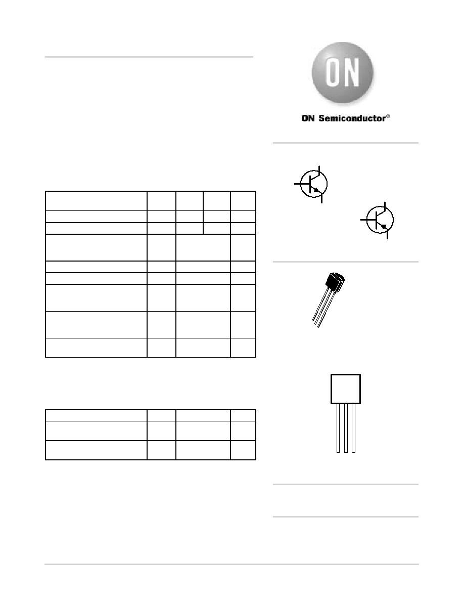
MARKING DIAGRAM
TO92
CASE 29
STYLE 1
1 2
3
See detailed ordering and shipping information in the package
dimensions section on page 123 of this data sheet.
ORDERING INFORMATION
http://onsemi.com
*For additional information on our PbFree strategy
and soldering details, please download the
ON Semiconductor Soldering and Mounting
Techniques Reference Manual, SOLDERRM/D.
COLLECTOR
3
2
BASE
1
EMITTER
COLLECTOR
3
2
BASE
1
EMITTER
NPN
PNP
相关PDF资料 |
PDF描述 |
|---|---|
| 2N6517RLRP | 500 mA, 350 V, NPN, Si, SMALL SIGNAL TRANSISTOR, TO-92 |
| 2N6516RL | 500 mA, 300 V, NPN, Si, SMALL SIGNAL TRANSISTOR, TO-92 |
| 2N6516RLRA | 500 mA, 300 V, NPN, Si, SMALL SIGNAL TRANSISTOR, TO-92 |
| 2N6516TA | 500 mA, 300 V, NPN, Si, SMALL SIGNAL TRANSISTOR, TO-92 |
| 2N6517STOF | 500 mA, 350 V, NPN, Si, SMALL SIGNAL TRANSISTOR |
相关代理商/技术参数 |
参数描述 |
|---|---|
| 2N6515RLRM | 功能描述:两极晶体管 - BJT 500mA 250V NPN RoHS:否 制造商:STMicroelectronics 配置: 晶体管极性:PNP 集电极—基极电压 VCBO: 集电极—发射极最大电压 VCEO:- 40 V 发射极 - 基极电压 VEBO:- 6 V 集电极—射极饱和电压: 最大直流电集电极电流: 增益带宽产品fT: 直流集电极/Base Gain hfe Min:100 A 最大工作温度: 安装风格:SMD/SMT 封装 / 箱体:PowerFLAT 2 x 2 |
| 2N6515RLRMG | 功能描述:两极晶体管 - BJT 500mA 250V NPN RoHS:否 制造商:STMicroelectronics 配置: 晶体管极性:PNP 集电极—基极电压 VCBO: 集电极—发射极最大电压 VCEO:- 40 V 发射极 - 基极电压 VEBO:- 6 V 集电极—射极饱和电压: 最大直流电集电极电流: 增益带宽产品fT: 直流集电极/Base Gain hfe Min:100 A 最大工作温度: 安装风格:SMD/SMT 封装 / 箱体:PowerFLAT 2 x 2 |
| 2N6515TA | 功能描述:两极晶体管 - BJT TO-92 RoHS:否 制造商:STMicroelectronics 配置: 晶体管极性:PNP 集电极—基极电压 VCBO: 集电极—发射极最大电压 VCEO:- 40 V 发射极 - 基极电压 VEBO:- 6 V 集电极—射极饱和电压: 最大直流电集电极电流: 增益带宽产品fT: 直流集电极/Base Gain hfe Min:100 A 最大工作温度: 安装风格:SMD/SMT 封装 / 箱体:PowerFLAT 2 x 2 |
| 2N6516 | 制造商:CENTRAL 制造商全称:Central Semiconductor Corp 功能描述:Small Signal Transistors |
| 2N6516BU | 功能描述:两极晶体管 - BJT TO-92 RoHS:否 制造商:STMicroelectronics 配置: 晶体管极性:PNP 集电极—基极电压 VCBO: 集电极—发射极最大电压 VCEO:- 40 V 发射极 - 基极电压 VEBO:- 6 V 集电极—射极饱和电压: 最大直流电集电极电流: 增益带宽产品fT: 直流集电极/Base Gain hfe Min:100 A 最大工作温度: 安装风格:SMD/SMT 封装 / 箱体:PowerFLAT 2 x 2 |
发布紧急采购,3分钟左右您将得到回复。