- 您现在的位置:买卖IC网 > PDF目录48161 > 2SK2613 8 A, 1000 V, 1.7 ohm, N-CHANNEL, Si, POWER, MOSFET PDF资料下载
参数资料
| 型号: | 2SK2613 |
| 元件分类: | JFETs |
| 英文描述: | 8 A, 1000 V, 1.7 ohm, N-CHANNEL, Si, POWER, MOSFET |
| 封装: | LEAD FREE, 2-16C1B, 3 PIN |
| 文件页数: | 1/6页 |
| 文件大小: | 201K |
| 代理商: | 2SK2613 |
2SK2613
2010-01-29
1
TOSHIBA Field Effect Transistor Silicon N Channel MOS Type (
π-MOSIII)
2SK2613
Switching Regulator Applications, DC-DC Converter and
Motor Drive Applications
Low drain-source ON-resistance: RDS (ON) = 1.4 (typ.)
High forward transfer admittance: Yfs = 6.0 S (typ.)
Low leakage current: IDSS = 100 μA (max) (VDS = 800 V)
Enhancement-model: Vth = 2.0 to 4.0 V (VDS = 10 V, ID = 1 mA)
Absolute Maximum Ratings (Ta = 25°C)
Characteristics
Symbol
Rating
Unit
Drain-source voltage
VDSS
1000
V
Drain-gate voltage (RGS = 20 kΩ)
VDGR
1000
V
Gate-source voltage
VGSS
±30
V
DC
(Note 1)
ID
8
Drain current
Pulse
(Note 1)
IDP
24
A
Drain power dissipation (Tc
= 25°C)
PD
150
W
Single pulse avalanche energy
(Note 2)
EAS
910
mJ
Avalanche current
IAR
8
A
Repetitive avalanche energy (Note 3)
EAR
15
mJ
Channel temperature
Tch
150
°C
Storage temperature range
Tstg
55 to 150
°C
Note: Using continuously under heavy loads (e.g. the application of high temperature/current/voltage and the significant change in
temperature, etc.) may cause this product to decrease in the reliability significantly even if the operating conditions (i.e.
operating temperature/current/voltage, etc.) are within the absolute maximum ratings. Please design the appropriate
reliability upon reviewing the Toshiba Semiconductor Reliability Handbook (“Handling Precautions”/“Derating Concept and
Methods”) and individual reliability data (i.e. reliability test report and estimated failure rate, etc).
Thermal Characteristics
Characteristics
Symbol
Max
Unit
Thermal resistance, channel to case
Rth (ch-c)
0.833
°C/W
Thermal resistance, channel to ambient
Rth (ch-a)
50
°C/W
Note 1: Please use devices on condition that the channel temperature is below 150°C.
Note 2: VDD = 90 V, Tch = 25°C, L = 26.3 mH, RG = 25 Ω, IAR = 8 A
Note 3: Repetitive rating: Pulse width limited by max junction temperature
This transistor is an electrostatic sensitive device. Please handle with caution.
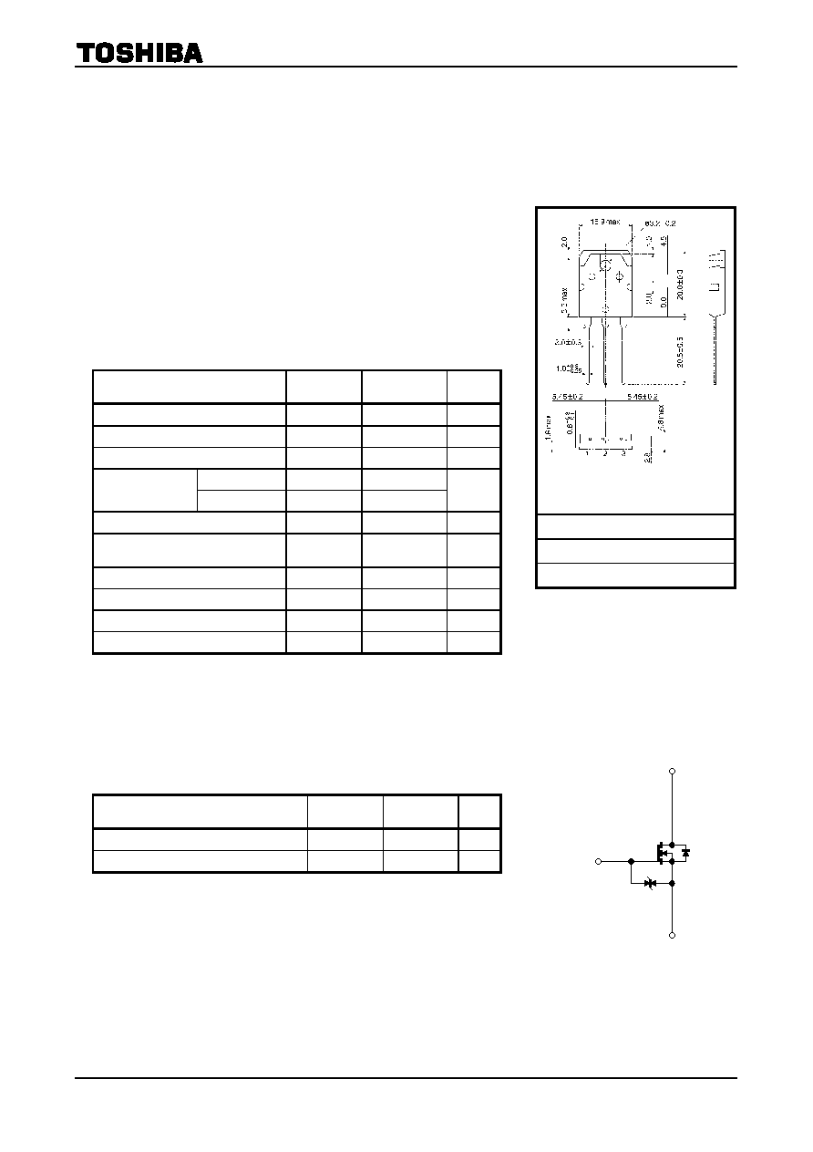
Unit: mm
1. GATE
2. DRAIN (HEAT SINK)
3. SOURSE
JEDEC
―
JEITA
―
TOSHIBA
216C1B
Weight: 4.6 g (typ.)
1
3
2
相关PDF资料 |
PDF描述 |
|---|---|
| 2SK2614(2-7B5B) | 20 A, 50 V, 0.046 ohm, N-CHANNEL, Si, POWER, MOSFET |
| 2SK2723 | 25 A, 60 V, 0.06 ohm, N-CHANNEL, Si, POWER, MOSFET |
| 2SK2802 | SMALL SIGNAL, FET |
| 2SK2846 | 2 A, 600 V, 5 ohm, N-CHANNEL, Si, POWER, MOSFET |
| 2SK2854 | UHF BAND, Si, N-CHANNEL, RF SMALL SIGNAL, MOSFET |
相关代理商/技术参数 |
参数描述 |
|---|---|
| 2SK2613(F) | 功能描述:MOSFET MOSFET N-Ch 1000V 8A Rdson 1.7 Ohm RoHS:否 制造商:STMicroelectronics 晶体管极性:N-Channel 汲极/源极击穿电压:650 V 闸/源击穿电压:25 V 漏极连续电流:130 A 电阻汲极/源极 RDS(导通):0.014 Ohms 配置:Single 最大工作温度: 安装风格:Through Hole 封装 / 箱体:Max247 封装:Tube |
| 2SK2614 | 功能描述:MOSFET N-Ch 50V 20A Rdson 0.046 Ohm RoHS:否 制造商:STMicroelectronics 晶体管极性:N-Channel 汲极/源极击穿电压:650 V 闸/源击穿电压:25 V 漏极连续电流:130 A 电阻汲极/源极 RDS(导通):0.014 Ohms 配置:Single 最大工作温度: 安装风格:Through Hole 封装 / 箱体:Max247 封装:Tube |
| 2SK2614(Q) | 功能描述:MOSFET N-Ch 50V 20A Rdson 0.046 Ohm RoHS:否 制造商:STMicroelectronics 晶体管极性:N-Channel 汲极/源极击穿电压:650 V 闸/源击穿电压:25 V 漏极连续电流:130 A 电阻汲极/源极 RDS(导通):0.014 Ohms 配置:Single 最大工作温度: 安装风格:Through Hole 封装 / 箱体:Max247 封装:Tube |
| 2SK2614(TE16L1) | 制造商:Toshiba America Electronic Components 功能描述:Trans MOSFET N-CH 50V 20A 3-Pin(2+Tab) Case DP T/R |
| 2SK2614(TE16L1,Q) | 制造商:Toshiba America Electronic Components 功能描述:Trans MOSFET N-CH 50V 20A 3-Pin(2+Tab) Case DP T/R 制造商:Toshiba 功能描述:Trans MOSFET N-CH 50V 20A 3-Pin (2+Tab) DP T/R Cut Tape 制造商:Toshiba America Electronic Components 功能描述:MOSFET N-CH 50V 20A DP |
发布紧急采购,3分钟左右您将得到回复。