- 您现在的位置:买卖IC网 > Datasheet目录378 > 2V7002WT1G (ON Semiconductor)MOSFET N-CH 60V 310MA SC70-3 Datasheet资料下载
参数资料
| 型号: | 2V7002WT1G |
| 厂商: | ON Semiconductor |
| 文件页数: | 1/5页 |
| 文件大小: | 0K |
| 描述: | MOSFET N-CH 60V 310MA SC70-3 |
| 标准包装: | 3,000 |
| FET 型: | MOSFET N 通道,金属氧化物 |
| FET 特点: | 逻辑电平门 |
| 漏极至源极电压(Vdss): | 60V |
| 电流 - 连续漏极(Id) @ 25° C: | 310mA |
| 开态Rds(最大)@ Id, Vgs @ 25° C: | 1.6 欧姆 @ 500mA,10V |
| Id 时的 Vgs(th)(最大): | 2.5V @ 250µA |
| 闸电荷(Qg) @ Vgs: | 700nC @ 10V |
| 输入电容 (Ciss) @ Vds: | 24.5pF @ 20V |
| 功率 - 最大: | 280mW |
| 安装类型: | 表面贴装 |
| 封装/外壳: | SC-70,SOT-323 |
| 供应商设备封装: | SC-70-3(SOT323) |
| 包装: | 带卷 (TR) |
�� �
�
�2N7002W,� 2V7002W�
�Small� Signal� MOSFET�
�60� V,� 340� mA,� Single,� N� ?� Channel,� SC� ?� 70�
�Features�
�?� ESD� Protected�
�?� Low� R� DS(on)�
�?� Small� Footprint� Surface� Mount� Package�
�?� These� Devices� are� Pb� ?� Free,� Halogen� Free/BFR� Free� and� are� RoHS�
�Compliant�
�?� 2V� Prefix� for� Automotive� and� Other� Applications� Requiring� Unique�
�Site� and� Control� Change� Requirements;� AEC� ?� Q101� Qualified� and�
�PPAP� Capable�
�V� (BR)DSS�
�60� V�
�http://onsemi.com�
�R� DS(on)� MAX�
�1.6� W� @� 10� V�
�2.5� W� @� 4.5� V�
�I� D� MAX�
�(Note� 1)�
�340� mA�
�Applications�
�?� Low� Side� Load� Switch�
�?� Level� Shift� Circuits�
�?� DC� ?� DC� Converter�
�?� Portable� Applications� i.e.� DSC,� PDA,� Cell� Phone,� etc.�
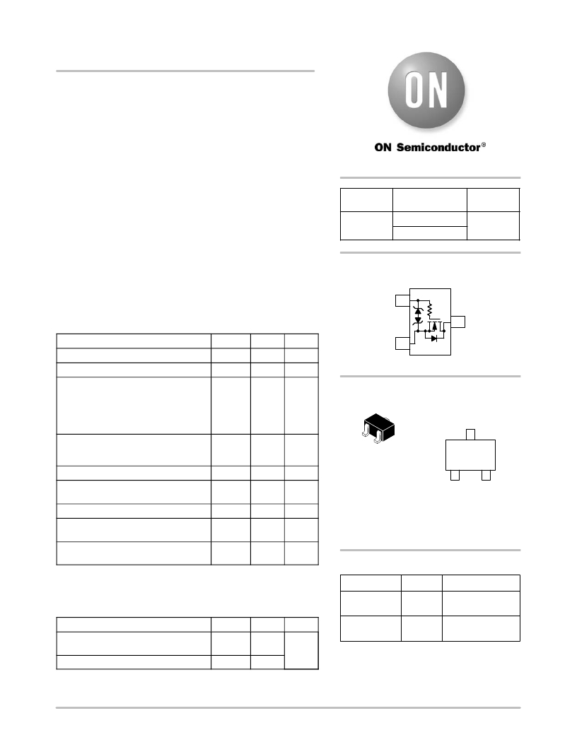
�SIMPLIFIED� SCHEMATIC�
�Gate� 1�
�MAXIMUM� RATINGS� (T� J� =� 25� °� C� unless� otherwise� stated)�
�3�
�Drain�
�Rating�
�Drain� ?� to� ?� Source� Voltage�
�Gate� ?� to� ?� Source� Voltage�
�Symbol�
�V� DSS�
�V� GS�
�Value�
�60�
�±� 20�
�Unit�
�V�
�V�
�Source�
�2�
�(Top� View)�
�Drain� Current� (Note� 1)�
�Steady� State�
�t<5s�
�T� A� =� 25� °� C�
�T� A� =� 85� °� C�
�T� A� =� 25� °� C�
�T� A� =� 85� °� C�
�I� D�
�310�
�220�
�340�
�240�
�mA�
�MARKING� DIAGRAM�
�&� PIN� ASSIGNMENT�
�Drain�
�3�
�Power� Dissipation� (Note� 1)�
�Steady� State�
�t<5s�
�Pulsed� Drain� Current� (t� p� =� 10� m� s)�
�Operating� Junction� and� Storage�
�Temperature� Range�
�P� D�
�I� DM�
�T� J� ,� T� STG�
�280�
�330�
�1.4�
�?� 55� to�
�+150�
�mW�
�A�
�°� C�
�SC� ?� 70/SOT� ?� 323�
�CASE� 419�
�STYLE� 8�
�1�
�Gate�
�71� M� G�
�G�
�2�
�Source�
�Source� Current� (Body� Diode)�
�Lead� Temperature� for� Soldering� Purposes�
�(1/8� ″� from� case� for� 10� s)�
�I� S�
�T� L�
�250�
�260�
�mA�
�°� C�
�71� =� Device� Code�
�M� =� Date� Code�
�G� =� Pb� ?� Free� Package�
�(Note:� Microdot� may� be� in� either� location)�
�Gate� ?� Source� ESD� Rating� ESD� 900� V�
�(HBM,� Method� 3015)�
�Stresses� exceeding� Maximum� Ratings� may� damage� the� device.� Maximum�
�Ratings� are� stress� ratings� only.� Functional� operation� above� the� Recommended�
�Operating� Conditions� is� not� implied.� Extended� exposure� to� stresses� above� the�
�Recommended� Operating� Conditions� may� affect� device� reliability.�
�THERMAL� CHARACTERISTICS�
�Characteristic� Symbol� Max� Unit�
�Junction� ?� to� ?� Ambient� ?� Steady� State� R� q� JA� 450� °� C/W�
�(Note� 1)�
�Junction� ?� to� ?� Ambient� ?� t� ≤� 5� s� (Note� 1)� R� q� JA� 375�
�1.� Surface� ?� mounted� on� FR4� board� using� 1� in� sq� pad� size� (Cu� area� =� 1.127� in�
�sq� [1� oz]� including� traces)�
�ORDERING� INFORMATION�
�Device� Package� Shipping� ?�
�2N7002WT1G� SC� ?� 70� 3000/Tape� &� Reel�
�(Pb� ?� Free)�
�2V7002WT1G� SC� ?� 70� 3000/Tape� &� Reel�
�(Pb� ?� Free)�
�?For� information� on� tape� and� reel� specifications,�
�including� part� orientation� and� tape� sizes,� please�
�refer� to� our� Tape� and� Reel� Packaging� Specifications�
�Brochure,� BRD8011/D.�
�?� Semiconductor� Components� Industries,� LLC,� 2012�
�September,� 2012� ?� Rev.� 5�
�1�
�Publication� Order� Number:�
�2N7002W/D�
�相关PDF资料 |
PDF描述 |
|---|---|
| 30 PSI-G-4V | SENSOR 30PSIG 4V DUAL |
| 3003308 | SHIELDING TAPE COPPER 8MMX33M |
| 3003310 | SHIELDING TAPE COPPER 10MMX33M |
| 3003320 | SHIELDING TAPE COPPER 20MMX33M |
| 3003325 | SHIELDING TAPE COPPER 25MMX33M |
相关代理商/技术参数 |
参数描述 |
|---|---|
| 2V7BC | 制造商:SEMTECH_ELEC 制造商全称:SEMTECH ELECTRONICS LTD. 功能描述:Silicon Epitaxial Planar Zener Diodes |
| 2V7BCA | 制造商:SEMTECH_ELEC 制造商全称:SEMTECH ELECTRONICS LTD. 功能描述:Silicon Epitaxial Planar Zener Diodes |
| 2V7BCB | 制造商:SEMTECH_ELEC 制造商全称:SEMTECH ELECTRONICS LTD. 功能描述:Silicon Epitaxial Planar Zener Diodes |
| 2V7BS | 制造商:SEMTECH_ELEC 制造商全称:SEMTECH ELECTRONICS LTD. 功能描述:SILICON PLANAR ZENER DIODES |
| 2V7BSA | 制造商:SEMTECH_ELEC 制造商全称:SEMTECH ELECTRONICS LTD. 功能描述:SILICON PLANAR ZENER DIODES |
发布紧急采购,3分钟左右您将得到回复。