- 您现在的位置:买卖IC网 > PDF目录33843 > 4X16E83VTW-6 (Electronic Theatre Controls, Inc.) 4 MEG x 16 EDO DRAM PDF资料下载
参数资料
| 型号: | 4X16E83VTW-6 |
| 厂商: | Electronic Theatre Controls, Inc. |
| 英文描述: | 4 MEG x 16 EDO DRAM |
| 中文描述: | 4迈可× 16 EDO公司的DRAM |
| 文件页数: | 19/24页 |
| 文件大小: | 598K |
| 代理商: | 4X16E83VTW-6 |
4
the upper byte (DQ8-DQ15). General byte and word
access timing is shown in Figures 1 and 2.
A logic HIGH on WE# dictates read mode, while a
logic LOW on WE# dictates write mode. During a
WRITE cycle, data-in (D) is latched by the falling edge
of WE or CAS# (CASL# or CASH#), whichever occurs
last. An EARLY WRITE occurs when WE is taken LOW
prior to either CAS# falling. A LATE WRITE or READ-
MODIFY-WRITE occurs when WE falls after CAS# (CASL#
or CASH#) is taken LOW. During EARLY WRITE cycles,
the data outputs (Q) will remain High-Z, regardless of
the state of OE#. During LATE WRITE or READ-MODIFY-
WRITE cycles, OE# must be taken HIGH to disable the
data outputs prior to applying input data. If a LATE
WRITE or READ-MODIFY-WRITE is attempted while
keeping OE# LOW, no write will occur, and the data
outputs will drive read data from the accessed location.
Additionally, both bytes must always be of the same
mode of operation if both bytes are active. A CAS#
precharge must be satisfied prior to changing modes of
operation between the upper and lower bytes. For
example, an EARLY WRITE on one byte and a LATE
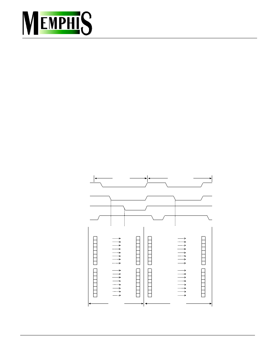
Figure 2
WORD and BYTE READ Example
STORED
DATA
1
0
1
RAS#
CASL#
WE#
Z = High-Z
ADDRESS 1
ADDRESS 0
0
1
0
1
0
WORD READ
LOWER BYTE READ
STORED
DATA
1
0
1
CASH#
OUTPUT
DATA
1
0
1
STORED
DATA
1
0
1
Z
OUTPUT
DATA
1
0
1
OUTPUT
DATA
1
0
1
OUTPUT
DATA
1
0
1
STORED
DATA
1
0
1
UPPER BYTE
(DQ8-DQ15)
OF WORD
LOWER BYTE
(DQ0-DQ7)
OF WORD
0
1
0
1
0
1
0
1
0
Z
0
1
0
1
0
1
0
1
0
WRITE on the other byte are not allowed during the
same cycle. However, an EARLY WRITE on one byte and
a LATE WRITE on the other byte, after a CAS# precharge
has been satisfied, are permissible.
EDO PAGE MODE
DRAM READ cycles have traditionally turned the
output buffers off (High-Z) with the rising edge of
CAS#. If CAS# went HIGH and OE# was LOW (active),
the output buffers would be disabled. The 64Mb EDO
DRAM offers an accelerated page mode cycle by elimi-
nating output disable from CAS# HIGH. This option is
called EDO, and it allows CAS# precharge time (tCP) to
occur without the output data going invalid (see READ
and EDO-PAGE-MODE READ waveforms).
EDO operates like any DRAM READ or FAST-PAGE-
MODE READ, except data is held valid after CAS# goes
HIGH, as long as RAS# and OE# are held LOW and WE#
is held HIGH. OE# can be brought LOW or HIGH while
CAS# and RAS# are LOW, and the DQs will transition
between valid data and High-Z. Using OE#, there are
DRAM ACCESS (continued)
4 MEG x 16
EDO DRAM
相关PDF资料 |
PDF描述 |
|---|---|
| 4X16E83V | 4 MEG x 16 EDO DRAM |
| 5-1437508-1 | TRANSISTOR SOCKET |
| 5-1437508-8 | TO-5, TRANSISTOR SOCKET |
| 5-1437515-1 | IC SOCKET |
| 5-1437515-3 | IC SOCKET |
相关代理商/技术参数 |
参数描述 |
|---|---|
| 4X2 | 制造商:Arcolectric 功能描述: |
| 4-X-2 | 制造商:Eaton Corporation 功能描述:COUNTER |
| 4X2.5PVC | 制造商:Nexans 功能描述:CABLE, SWA, PVCORE, 4CORE, 2.5MM, 100M |
| 4X22 AWG YELLOW PUR S3090 | 制造商:TURCK Inc 功能描述:4X22 AWG YELLOW PUR S3090 |
| 4X2A | 制造商:Eaton Corporation 功能描述:4 Digit Pushbutton Stroke Counter, Knob Reset |
发布紧急采购,3分钟左右您将得到回复。