- 您现在的位置:买卖IC网 > PDF目录156848 > 514NBBXXXXXXBAGR (SILICON LABORATORIES) 170 MHz, OTHER CLOCK GENERATOR, PDSO6 PDF资料下载
参数资料
| 型号: | 514NBBXXXXXXBAGR |
| 厂商: | SILICON LABORATORIES |
| 元件分类: | 时钟产生/分配 |
| 英文描述: | 170 MHz, OTHER CLOCK GENERATOR, PDSO6 |
| 封装: | 3.20 X 5 MM, ROHS COMPLIANT PACKAGE-6 |
| 文件页数: | 5/32页 |
| 文件大小: | 267K |
| 代理商: | 514NBBXXXXXXBAGR |
第1页第2页第3页第4页当前第5页第6页第7页第8页第9页第10页第11页第12页第13页第14页第15页第16页第17页第18页第19页第20页第21页第22页第23页第24页第25页第26页第27页第28页第29页第30页第31页第32页
Si514
Preliminary Rev. 0.9
13
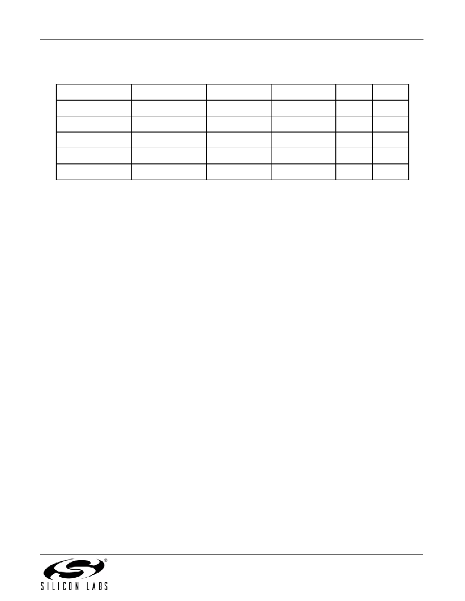
6. Determine values for LP1 and LP2 according to Table 10:
7. Write new LP1, LP2, M_Frac, M_Int, HS_DIV and LS_DIV register values (be sure to write M_Int[8:3] (Register
9) after writing to the M_Frac registers (Registers 5-8)
8. Write FCAL (Register 132, bit 0) to a 1 (this bit auto-resets, so it will always read as 0).
9. Enable the output: Write OE register bit to a 1.
The Si514 does not automatically detect large frequency changes. The user needs to assert the FCAL register bit
to initiate the calibration cycle required to re-center the VCO around the new frequency. Large frequency changes
are discontinuous and output may skip to intermediate frequencies or generate glitches. Resetting the OE bit
before FCAL will prevent intermediate frequencies from appearing on the output while Si514 completes a
calibration cycle and settles to F'CENTER. Settling time for large frequency changes is 10 msec maximum.
Example 2.2:
The user has a part that is programmed with SPEED_GRADE_MIN = 20 and SPEED_GRADE_MAX = 250 that is
programmed from the factory for FOUT = 50 MHz and wants to change to an STS-1 rate of 51.84 MHz. This
represents a change of +36,800 ppm which exceeds ±1000 ppm and therefore requires a large frequency change
process.
1. Write Reg 132, bit 2 to a 0 to disable the output.
2. Since 51.84 MHz is not in Table 2.1, the divider parameters must be calculated.
3. Calculate LS_DIV by using Eq 2.7:
a. LS_DIV = 2080/(51.84 x 1022) = 0.039
b. Since 0.039 < 1, use a divide-by-one (bypass), therefore LS_DIV = 0
4. Calculate HS_DIV(MIN) by using Eq 2.9:
a. HS_DIV(MIN) = 2080/(51.84 x 1) = 40.123
b. Since 40.123 > 40, use HS_DIV(MIN) = 42 = 0x2A
5. From Eq 2.11:
a. M = 1 x 42 x 51.84/31.98 = 68.08255159474
b. M_Int = 68 = 0x44
c. M_Frac = 0.08255259474 x 229 = 44,320,087 = 0x2A44557
6. From Table 2.2:
a. LP1 = 3
b. LP2 = 3
7. Write Registers 0, 5-11:
a. Register 0 = 0x33
b. Register 5 = 0x57 (M_Frac[7:0])
c. Register 6 = 0x45 (M_Frac[15:8])
Table 10. LP1, LP2 Values
Fvco_max
Fvco_min
M_max
M_min
LP1
LP2
2500000000.00000
2425467616.18572
78.173858662
75.843265046
4
2425467616.18572
2332545246.89005
75.843265046
72.937624981
3
4
2332545246.89005
2170155235.53450
72.937624981
67.859763463
3
2170155235.53450
2087014168.27005
67.859763463
65.259980246
2
3
2087014168.27005
2080000000.00000
65.259980246
65.040650407
2
相关PDF资料 |
PDF描述 |
|---|---|
| 514NBCXXXXXXBAG | 125 MHz, OTHER CLOCK GENERATOR, PDSO6 |
| 514NCAXXXXXXBAG | 250 MHz, OTHER CLOCK GENERATOR, PDSO6 |
| 514NCBXXXXXXAAGR | 170 MHz, OTHER CLOCK GENERATOR, PDSO6 |
| 514NCBXXXXXXAAG | 170 MHz, OTHER CLOCK GENERATOR, PDSO6 |
| 514NCCXXXXXXBAGR | 125 MHz, OTHER CLOCK GENERATOR, PDSO6 |
相关代理商/技术参数 |
参数描述 |
|---|---|
| 514NCA000208AAG | 制造商:Silicon Laboratories Inc 功能描述:OSCILLATOR - Trays |
| 514NCA000208AAGR | 制造商:Silicon Laboratories Inc 功能描述:OSCILLATOR - Tape and Reel |
| 514NCA000688BAG | 功能描述:标准时钟振荡器 PROGRMABLE XO 6 PIN 0.7PS RS JTR RoHS:否 制造商:AVX 产品:Standard Clock Oscillators 封装 / 箱体:7 mm x 5 mm 频率:75 MHz 频率稳定性:50 PPM 电源电压:2.5 V 负载电容: 端接类型:SMD/SMT 最小工作温度:0 C 最大工作温度:+ 70 C 输出格式:LVDS 尺寸: 封装:Reel 系列: |
| 514NCA000688BAGR | 制造商:Silicon Laboratories Inc 功能描述:OSCILLATOR - Tape and Reel |
| 514NCA000776AAG | 制造商:Silicon Laboratories Inc 功能描述:OSCILLATOR - Trays |
发布紧急采购,3分钟左右您将得到回复。