- 您现在的位置:买卖IC网 > PDF目录97779 > 5962-0722301VFA (TEXAS INSTRUMENTS INC) OP-AMP, 5500 uV OFFSET-MAX, 3000 MHz BAND WIDTH, CDFP16 PDF资料下载
参数资料
| 型号: | 5962-0722301VFA |
| 厂商: | TEXAS INSTRUMENTS INC |
| 元件分类: | 运算放大器 |
| 英文描述: | OP-AMP, 5500 uV OFFSET-MAX, 3000 MHz BAND WIDTH, CDFP16 |
| 封装: | CERAMIC, CFP-16 |
| 文件页数: | 16/30页 |
| 文件大小: | 1043K |
| 代理商: | 5962-0722301VFA |
第1页第2页第3页第4页第5页第6页第7页第8页第9页第10页第11页第12页第13页第14页第15页当前第16页第17页第18页第19页第20页第21页第22页第23页第24页第25页第26页第27页第28页第29页第30页
www.ti.com
VS+
CM
VSignal
VS-
RF
RG
RT
RO
VOUT+
VOUT-
THS 4513
RS
RT
RS
VS+
RPU
2.7pF
0.1 F
m
14 Bit,
125 MSPS
A IN +
A IN - CM
ADS5500
4 V
THS 4513
CM
348 W
100 W
69.8 W
VIN
From
50
Source
W
100 W
-1 V
69.8 W
.
49.9 W
0.22 F
m
49
.9 W
0.22 F
m
0.22 F
m
0.1 F
m
V S+= 3Vto 5V
CM
V Signal
V S-
R F
R G
R T
R O
V OUT+
V OUT-
THS
C
R S
R T
C
R S
C
THS4513 + ADS5500 Combined Performance
THS4513 + ADS5424 Combined Performance
SLOS539A – SEPTEMBER 2007 – REVISED OCTOBER 2007
impedance, termination, and 348
feedback resistor.
Refer to Table 3 for component values to set proper
50
termination for other common gains. A split
power supply of 4 V and –1 V is used to set the input
and output common-mode voltages to approximately
mid-supply while setting the input common-mode of
the ADS5500 to the recommended 1.55 V. This
maintains
maximum
headroom
on
the
internal
transistors of the THS4513 to ensure optimum
performance.
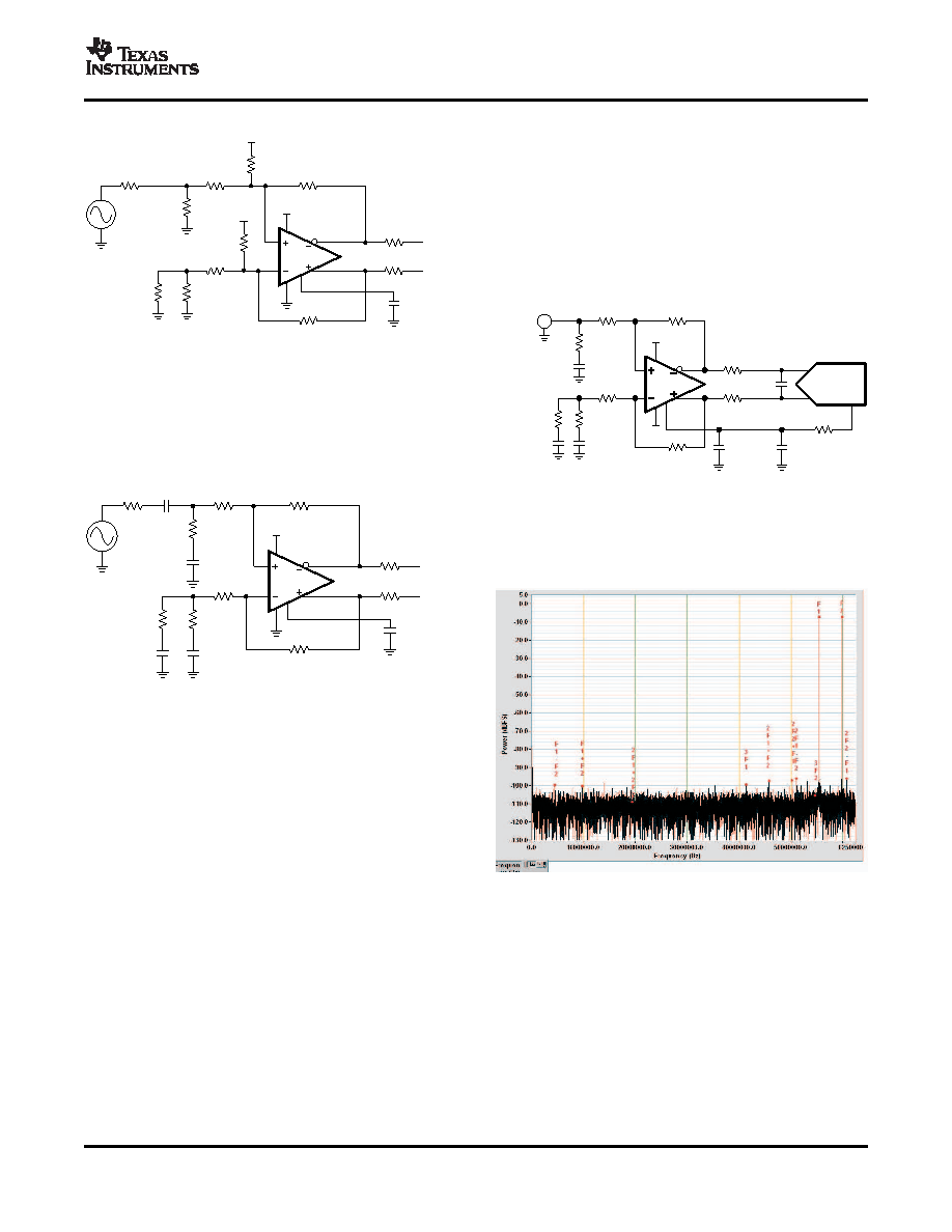
Figure 64. THS4513 DC Coupled Single-Supply
With RPU Used to Set VIC
Figure 65 shows AC coupling to the source. Using
capacitors in series with the termination resistors
allows the amplifier to self-bias both input and output
to mid-supply.
Figure 66. THS4513 + ADS5500 Circuit
Figure 67 shows the 2-tone FFT of the THS4513 +
ADS5500 circuit with 65 MHz and 70 MHz input
frequencies. The SFDR is 90 dBc.
Figure 65. THS4513 AC Coupled Single-Supply
The THS4513 is designed to be a high-performance
drive amplifier for high-performance data converters
like the ADS5500 14 bit 125 MSPS ADC. Figure 66
shows a circuit combining the two devices. The
THS4513 amplifier circuit provides 10 dB of gain,
converts the single-ended input to differential, and
sets the proper input common-mode voltage to the
ADS5500. The 100
resistors and 2.7 pF capacitor
Figure 67. THS4513 + ADS5500 2-Tone FFT With
between the THS4513 outputs and ADS5500 inputs,
65 MHz and 70 MHz Input
along with the input capacitance of the ADS5500,
limit the bandwidth of the signal to 115 MHz (–3 dB).
For testing, a signal generator is used for the signal
source. The generator is an AC-coupled 50
source.
Figure 68 shows the THS4513 driving the ADS5424
A band-pass filter is inserted in series with the input
ADC.
to reduce harmonics and noise from the signal
The THS4513 amplifier provides 10 dB of gain,
source. Input termination is accomplished via the 69.8
converts the single-ended input to differential, and
resistor and 0.22 μF capacitor to ground in
sets the proper input common-mode voltage to the
conjunction with the input impedance of the amplifier
ADS5424. Input termination and circuit testing is the
circuit. A 0.22
μF capacitor and 49.9 resistor is
same as described above for the THS4513 +
inserted to ground across the 69.8
resistor and
ADS5500 circuit.
0.22
μF capacitor on the alternate input to balance
the
circuit.
Gain
is
a
function
of
the
source
Copyright 2007, Texas Instruments Incorporated
23
Product Folder Link(s): THS4513-SP
相关PDF资料 |
PDF描述 |
|---|---|
| 5962-7704301VCA | QUAD OP-AMP, 7000 uV OFFSET-MAX, 1.2 MHz BAND WIDTH, CDIP14 |
| 5962-86860012X | QUAD COMPARATOR, 5000 uV OFFSET-MAX, CQCC20 |
| 5962-8686001EX | QUAD COMPARATOR, 5000 uV OFFSET-MAX, 200 ns RESPONSE TIME, CDIP16 |
| 5962-8687701GA | COMPARATOR, 4000 uV OFFSET-MAX, 200 ns RESPONSE TIME, CQCC20 |
| 5962-8687701PA | COMPARATOR, 4000 uV OFFSET-MAX, 200 ns RESPONSE TIME, CQCC20 |
相关代理商/技术参数 |
参数描述 |
|---|---|
| 5962-0722401QXB | 制造商:ATMEL 制造商全称:ATMEL Corporation 功能描述:Rad-Hard 32 bit SPARC V8 Processor |
| 5962-0722901QXA | 功能描述:线性稳压器 - 标准 RoHS:否 制造商:STMicroelectronics 输出类型: 极性: 输出电压:1.8 V 输出电流:150 mA 负载调节: 最大输入电压:5.5 V 线路调整率: 最大工作温度:+ 125 C 安装风格:SMD/SMT 封装 / 箱体:SOT-323-5L |
| 5962-0722902QZA | 制造商:Texas Instruments 功能描述:MICROCIRCUIT, VOLTAGE REGULATOR - Rail/Tube |
| 5962-0723001VXC | 制造商:Texas Instruments 功能描述:HIGH PERFORMANCE CLOCK SYNC - Rail/Tube |
| 5962-0724701VXA | 功能描述:数模转换器- DAC 14B,2.4 GSPS DAC RoHS:否 制造商:Texas Instruments 转换器数量:1 DAC 输出端数量:1 转换速率:2 MSPs 分辨率:16 bit 接口类型:QSPI, SPI, Serial (3-Wire, Microwire) 稳定时间:1 us 最大工作温度:+ 85 C 安装风格:SMD/SMT 封装 / 箱体:SOIC-14 封装:Tube |
发布紧急采购,3分钟左右您将得到回复。