- 您现在的位置:买卖IC网 > PDF目录293971 > 5962-8981702ZX (CYPRESS SEMICONDUCTOR CORP) 32K X 8 UVPROM, 45 ns, CQCC32 PDF资料下载
参数资料
| 型号: | 5962-8981702ZX |
| 厂商: | CYPRESS SEMICONDUCTOR CORP |
| 元件分类: | PROM |
| 英文描述: | 32K X 8 UVPROM, 45 ns, CQCC32 |
| 封装: | CERAMIC, LCC-32 |
| 文件页数: | 1/11页 |
| 文件大小: | 245K |
| 代理商: | 5962-8981702ZX |
32K x 8 Power Switched and
Reprogrammable PROM
CY7C271
CY7C274
Cypress Semiconductor Corporation
3901 North First Street
San Jose
CA 95134
408-943-2600
Document #: 38-04008 Rev. *B
Revised December 27, 2002
1CY7C274
Features
CMOS for optimum speed/power
Windowed for reprogrammability
High speed
— 30 ns (Commercial)
— 35 ns (Military)
Low power
— 660 mW (commercial)
— 715 mW (military)
Super low standby power
— Less than 165 mW when deselected
EPROM technology 100% programmable
Slim 300-mil package (7C271)
Direct replacement for bipolar PROMs
Capable of withstanding >2001V static discharge
Functional Description
The
CY7C271
and
CY7C274
are
high-performance
32,768-word by 8-bit CMOS PROMs. When disabled (CE
HIGH), the 7C271/7C274 automatically powers down into a
low-power stand-by mode. The CY7C271 is packaged in the
300-mil slim package. The CY7C274 is packaged in the
industry standard 600-mil package. Both the CY7C271 and
CY7C274 are available in a cerDIP package equipped with an
erasure window to provide for reprogrammability. When
exposed to UV light, the PROM is erased and can be repro-
grammed. The memory cells utilize proven EPROM floating
gate technology and byte-wide intelligent programming
algorithms.
The CY7C271 and CY7C274 offer the advantage of lower
power, superior performance, and programming yield. The
EPROM cell requires only 12.5V for the super voltage, and low
current requirements allow for gang programming. The
EPROM cells allow each memory location to be tested 100%
because each location is written into, erased, and repeatedly
exercised prior to encapsulation. Each PROM is also tested
for AC performance to guarantee that after customer
programming, the product will meet DC and AC specification
limits.
Reading the 7C271 is accomplished by placing active LOW
signals on CS1 and CE, and an active HIGH on CS2. Reading the
7C274 is accomplished by placing active LOW signals on OE and
CE. The contents of the memory location addressed by the address
lines (A0A14) will become available on the output lines (O0O7).
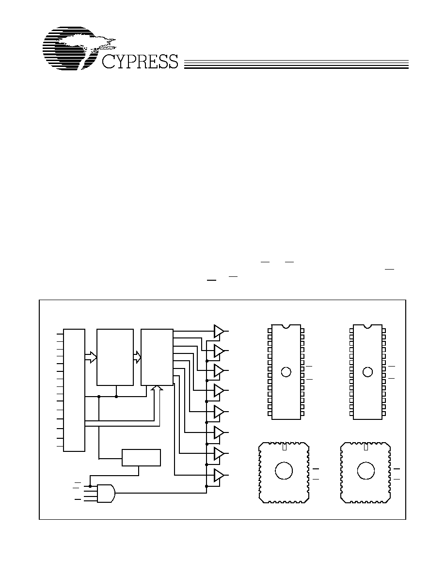
Logic Block Diagram
Pin Configurations
1
2
3
4
5
6
7
8
9
10
11
12
16
17
18
19
20
24
23
22
21
13
14
25
28
27
26
A8
A7
A6
A5
A4
A3
A2
A1
A0
O0
O1
O2
GND
VCC
A11
A12
A13
O7
O6
O4
O5
O3
A12
A11
A9
A8
A7
A6
A5
A4
A3
A2
A1
A0
POWER-DOWN
O7
O6
O5
O4
O3
O2
O1
O0
CE
256 x 1024
PROGRAMABLE
ARRAY
8 x 1 OF 128
MULTIPLEXER
12
31
4
5
6
7
8
9
10
32 1
30
13
14151617
26
25
24
23
22
21
11
V CC
A5
A4
A3
A2
A6
A1
A13
A14
O7
O6
O
4
GND
A12
A
7
A
8
O
3
O
1
181920
27
28
29
32
NC
O
5
NC
15
A10
A13
(7C271) CS1
(7C274) OE
A9
A10
A14
CS1
CS2
CE
A
9
A
10
A
11
CS1
CS2
O0
A14
1
2
3
4
5
6
7
8
9
10
11
12
16
17
18
19
20
24
23
22
21
13
14
25
28
27
26
12
31
4
5
6
7
8
9
10
32 1
30
13
14151617
26
25
24
23
22
21
11
A
7
V CC
A
12
181920
27
28
29
32
15
NC
A
14
A
13
A12
A7
A6
A5
A4
A3
A2
A1
A0
O0
O1
O2
GND
VCC
A13
A8
A9
O7
O6
O4
O5
O3
A9
A11
O7
O6
A8
VPP
A14
(7C271) CS2
7C271
7C274
NC
A11
OE
A10
CE
NC
CE
O
2
A0
NC
A5
A4
A3
A2
A6
A1
O0
A0
V
PP
NC
OE
A10
CE
O
4
GND
O
3
O
1
NC
O
5
O
2
DIP/Flatpack
LCC/PLCC (Opaque Only)
7C271
7C274
X ADDRESS
Y ADDRESS
LCC/PLCC (Opaque Only)
相关PDF资料 |
PDF描述 |
|---|---|
| 5962-9096301MYA | 19-BIT, DSP-FFT PROCESSOR, PPGA89 |
| 5962-9176201M3A | 8-BIT, DSP-PIPELINE REGISTER, QCC28 |
| 5962-9205803MYA | 32-BIT, 40 MHz, OTHER DSP, CQFP132 |
| 5962-9205805QXA | 32-BIT, 60 MHz, OTHER DSP, CPGA141 |
| 5962-9309101HYA | EEPROM 5V MODULE, CDIP32 |
相关代理商/技术参数 |
参数描述 |
|---|---|
| 5962-8981703XA | 制造商:QP Semiconductor 功能描述:EPROM UV 256K-Bit 32K x 8 35ns 28-Pin CDIP |
| 5962-8981704ZX | 制造商:Cypress Semiconductor 功能描述:EPROM UV 256K-Bit 32K x 8 55ns 32-Pin LCC |
| 5962-8981705UA | 制造商:Cypress Semiconductor 功能描述:32K X 8 POWER SWITCHED AND REPROGRAMMABLE PROM |
| 5962-8982101PA | 制造商:e2v technologies 功能描述:Pref DRVR Dual 4.5V to 15V 1133mW 8-Pin CDIP |
| 59628982303MZC | 制造商:XILINX 功能描述:xc3090-100cb164 |
发布紧急采购,3分钟左右您将得到回复。