- 您现在的位置:买卖IC网 > PDF目录91416 > 5962-9451203M2X (MAXIM INTEGRATED PRODUCTS INC) OP-AMP, 5000 uV OFFSET-MAX, CQCC20 PDF资料下载
参数资料
| 型号: | 5962-9451203M2X |
| 厂商: | MAXIM INTEGRATED PRODUCTS INC |
| 元件分类: | 运算放大器 |
| 英文描述: | OP-AMP, 5000 uV OFFSET-MAX, CQCC20 |
| 封装: | CERAMIC, LCC-20 |
| 文件页数: | 10/10页 |
| 文件大小: | 147K |
| 代理商: | 5962-9451203M2X |
DS4420
I2C Programmable-Gain Amplifier
for Audio Applications
_____________________________________________________________________
9
Byte Read: A byte read is an 8-bit information transfer
from the slave to the master plus a 1-bit ACK or NACK
from the master to the slave. The 8 bits of information
that are transferred (most significant bit first) from the
slave to the master are read by the master using the bit
read definition above, and the master transmits an ACK
using the bit write definition to receive additional data
bytes. The master must NACK the last byte read to ter-
minate communication so the slave will return control of
SDA to the master.
Slave Address Byte: Each slave on the I2C bus
responds to a slave address byte sent immediately fol-
lowing a start condition. The slave address byte con-
tains the slave address in the most significant 7 bits
and the R/W bit in the least significant bit.
The DS4420’s slave address is determined by the state
of the A0, A1, and A2 address pins as shown in Figure
2. Address pins connected to GND result in a ‘0’ in the
corresponding bit position in the slave address.
Conversely, address pins connected to VCC result in a
‘1’ in the corresponding bit positions.
When the R/W bit is 0 (such as in A0h), the master is indi-
cating it will write data to the slave. If R/W is set to a 1,
(A1h in this case), the master is indicating it wants to read
from the slave.
If an incorrect (nonmatching) slave address is written,
the DS4420 will assume the master is communicating
with another I2C device and ignore the communication
until the next start condition is sent.
Memory Address: During an I2C write operation to the
DS4420, the master must transmit a memory address to
identify the memory location where the slave is to store
the data. The memory address is always the second
byte transmitted during a write operation following the
slave address byte.
I2C Communication
Writing a Single Byte to a Slave: The master must gen-
erate a start condition, write the slave address byte (R/W
= 0), write the memory address, write the byte of data,
and generate a stop condition. The master must read the
slave’s acknowledgement during all byte write operations.
Reading a Single Byte from a Slave: Unlike the write
operation that uses the specified memory address byte
to define where the data is to be written, the read oper-
ation occurs at the present value of the memory
address counter. A dummy write cycle can be used to
force the address pointer to a desired location. To do
this, the master generates a start condition, writes the
slave address byte (R/W =0), writes the memory
address where it desires to read, generates a repeated
start condition, writes the slave address byte (R/W = 1),
reads the data byte with a NACK to indicate the end of
the transfer, and generates a stop condition.
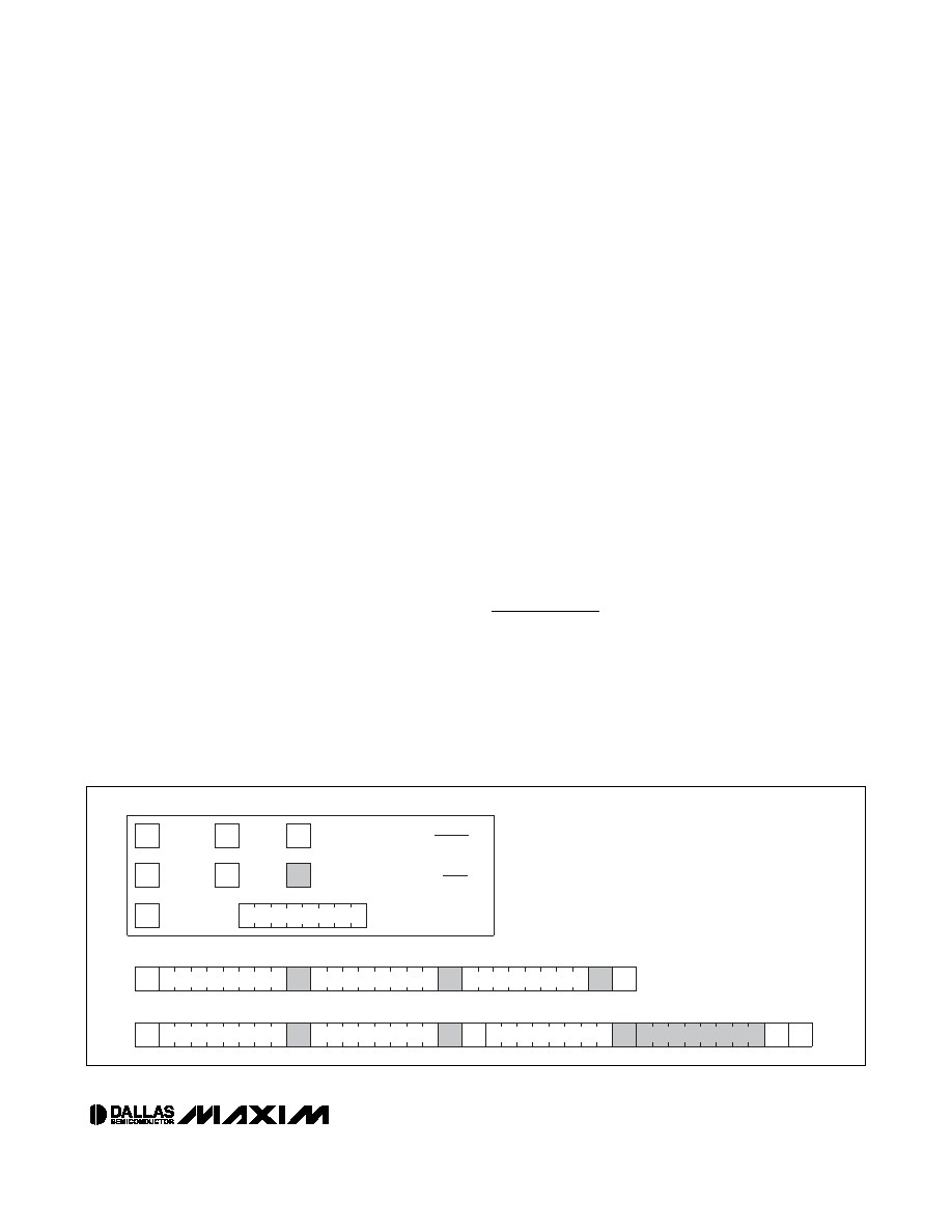
See Figure 4 for I2C communication examples.
Applications Information
Power-Supply Decoupling
The DS4420 has separate supply voltages for its ana-
log and digital circuitry. For best noise and distortion
performance, place a 0.1F or 0.01F capacitor from
VCC to GND and from AVCC to AGND. These capaci-
tors should be placed as close as possible to the sup-
ply and ground pins of the device.
XXXXXXXX
10
1
0
A0 0
A1
A2
11
1
0
1
10
1
0
A0 0
A1
A2
11
1
0
1
10
1
0
A0 1
A1
A2
COMMUNICATIONS KEY
WRITE THE GAIN SETTING
F8h
READ THE GAIN SETTING
F8h
8-BITS ADDRESS OR DATA
NOTE 2: THE FIRST BYTE SENT AFTER A START CONDITION IS
ALWAYS THE SLAVE ADDRESS FOLLOWED BY THE
READ/WRITE BIT.
START
ACK
NOT
ACK
S
A
AA
P
ASr
AN
P
REGISTER SETTING
A
PN
Sr
STOP
REPEATED
START
NOTE 1: ALL BYTES ARE SENT MOST SIGNIFICANT BIT FIRST.
SHADED BOXES INDICATE THE SLAVE IS
CONTROLLING SDA
WHITE BOXES INDICATE THE MASTER IS
CONTROLLING SDA
Figure 4. I2C Communication Examples
相关PDF资料 |
PDF描述 |
|---|---|
| 5962-9452001XX | OP-AMP, 2000 uV OFFSET-MAX, 1.6 MHz BAND WIDTH, MDFP14 |
| 5962-9452001XX | OP-AMP, 2000 uV OFFSET-MAX, 1.6 MHz BAND WIDTH, CDFP14 |
| 5962-9459701MPA | OP-AMP, CDIP8 |
| 5962-9460401MPA | DUAL OP-AMP, 350 uV OFFSET-MAX, 0.08 MHz BAND WIDTH, CDIP8 |
| 5962-9460401MPX | DUAL OP-AMP, 350 uV OFFSET-MAX, 0.08 MHz BAND WIDTH, CDIP8 |
相关代理商/技术参数 |
参数描述 |
|---|---|
| 5962-9451203MPA | 功能描述:视频放大器 RoHS:否 制造商:ON Semiconductor 通道数量:4 电源类型: 工作电源电压:3.3 V, 5 V 电源电流: 最小工作温度: 最大工作温度: 封装 / 箱体:TSSOP-14 封装:Reel |
| 5962-9451204MCA | 功能描述:视频放大器 CMOS Video MUX/Amplifier RoHS:否 制造商:ON Semiconductor 通道数量:4 电源类型: 工作电源电压:3.3 V, 5 V 电源电流: 最小工作温度: 最大工作温度: 封装 / 箱体:TSSOP-14 封装:Reel |
| 5962-9451301MPA | 制造商:Texas Instruments 功能描述:Current Mode PWM Controller 1A 8-Pin CDIP Tube 制造商:Rochester Electronics LLC 功能描述:- Bulk 制造商:Texas Instruments 功能描述:CURRENT MODE PWM CNTRLR 1A 8CDIP - Rail/Tube |
| 5962-9451302MPA | 制造商:Texas Instruments 功能描述:Current Mode PWM Controller 1A 8-Pin CDIP Tube 制造商:Rochester Electronics LLC 功能描述:- Bulk 制造商:Texas Instruments 功能描述:CURRENT MODE PWM CNTRLR 1A 8CDIP - Rail/Tube |
| 5962-9451303MPA | 制造商:Texas Instruments 功能描述:Current Mode PWM Controller 1A 8-Pin CDIP Tube |
发布紧急采购,3分钟左右您将得到回复。