- 您现在的位置:买卖IC网 > PDF目录91416 > 5962-9451203M2X (MAXIM INTEGRATED PRODUCTS INC) OP-AMP, 5000 uV OFFSET-MAX, CQCC20 PDF资料下载
参数资料
| 型号: | 5962-9451203M2X |
| 厂商: | MAXIM INTEGRATED PRODUCTS INC |
| 元件分类: | 运算放大器 |
| 英文描述: | OP-AMP, 5000 uV OFFSET-MAX, CQCC20 |
| 封装: | CERAMIC, LCC-20 |
| 文件页数: | 9/10页 |
| 文件大小: | 147K |
| 代理商: | 5962-9451203M2X |
DS4420
I2C Programmable-Gain Amplifier
for Audio Applications
8
_____________________________________________________________________
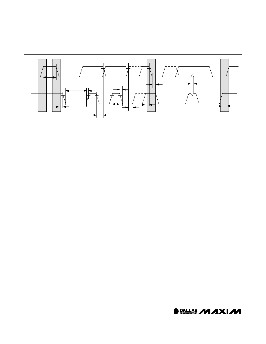
I2C Serial Interface Description
I2C Definitions
The following terminology is commonly used to
describe I2C data transfers. See the timing diagram
(Figure 3) and the
I2C AC Electrical Characteristics
table for additional information.
Master Device: The master device controls the slave
devices on the bus. The master device generates SCL
clock pulses, start and stop conditions.
Slave Devices: Slave devices send and receive data
at the master’s request.
Bus Idle or Not Busy: Time between stop and start
conditions when both SDA and SCL are inactive and in
their logic-high states.
Start Condition: A start condition is generated by the
master to initiate a new data transfer with a slave.
Transitioning SDA from high to low while SCL remains
high generates a start condition.
Stop Condition: A stop condition is generated by the
master to end a data transfer with a slave. Transitioning
SDA from low to high while SCL remains high gener-
ates a stop condition.
Repeated Start Condition: The master can use a
repeated start condition at the end of one data transfer
to indicate that it will immediately initiate a new data
transfer following the current one. Repeated starts are
commonly used during read operations to identify a
specific memory address to begin a data transfer. A
repeated start condition is issued identically to a nor-
mal start condition.
Bit Write: Transitions of SDA must occur during the low
state of SCL. The data on SDA must remain valid and
unchanged during the entire high pulse of SCL plus the
setup and hold time requirements. Data is shifted into
the device during the rising edge of the SCL.
Bit Read: At the end of a write operation, the master
must release the SDA bus line for the proper amount of
setup time before the next rising edge of SCL during a
bit read. The device shifts out each bit of data on SDA at
the falling edge of the previous SCL pulse and the data
bit is valid at the rising edge of the current SCL pulse.
Remember that the master generates all SCL clock
pulses including when it is reading bits from the slave.
Acknowledgement (ACK and NACK): An Acknowledge-
ment (ACK) or Not Acknowledge (NACK) is always the
9th bit transmitted during a byte transfer. The device
receiving data (the master during a read or the slave dur-
ing a write operation) performs an ACK by transmitting a
zero during the 9th bit. A device performs a NACK by
transmitting a one (done by releasing SDA) during the 9th
bit. Timing (Figure 3) for the ACK and NACK is identical to
all other bit writes. An ACK is the acknowledgment that
the device is properly receiving data. A NACK is used to
terminate a read sequence or as an indication that the
device is not receiving data.
Byte Write: A byte write consists of 8 bits of informa-
tion transferred from the master to the slave (most sig-
nificant bit first) plus a 1-bit acknowledgement from the
slave to the master. The 8 bits transmitted by the mas-
ter are done according to the bit write definition and the
acknowledgement is read using the bit read definition.
SDA
SCL
tHD:STA
tLOW
tHIGH
tR
tF
tBUF
tHD:DAT
tSU:DAT
REPEATED
START
tSU:STA
tHD:STA
tSU:STO
tSP
STOP
START
NOTE: TIMING IS REFERENCE TO VIL(MAX) AND VIH(MIN).
Figure 3. I2C Timing Diagram
相关PDF资料 |
PDF描述 |
|---|---|
| 5962-9452001XX | OP-AMP, 2000 uV OFFSET-MAX, 1.6 MHz BAND WIDTH, MDFP14 |
| 5962-9452001XX | OP-AMP, 2000 uV OFFSET-MAX, 1.6 MHz BAND WIDTH, CDFP14 |
| 5962-9459701MPA | OP-AMP, CDIP8 |
| 5962-9460401MPA | DUAL OP-AMP, 350 uV OFFSET-MAX, 0.08 MHz BAND WIDTH, CDIP8 |
| 5962-9460401MPX | DUAL OP-AMP, 350 uV OFFSET-MAX, 0.08 MHz BAND WIDTH, CDIP8 |
相关代理商/技术参数 |
参数描述 |
|---|---|
| 5962-9451203MPA | 功能描述:视频放大器 RoHS:否 制造商:ON Semiconductor 通道数量:4 电源类型: 工作电源电压:3.3 V, 5 V 电源电流: 最小工作温度: 最大工作温度: 封装 / 箱体:TSSOP-14 封装:Reel |
| 5962-9451204MCA | 功能描述:视频放大器 CMOS Video MUX/Amplifier RoHS:否 制造商:ON Semiconductor 通道数量:4 电源类型: 工作电源电压:3.3 V, 5 V 电源电流: 最小工作温度: 最大工作温度: 封装 / 箱体:TSSOP-14 封装:Reel |
| 5962-9451301MPA | 制造商:Texas Instruments 功能描述:Current Mode PWM Controller 1A 8-Pin CDIP Tube 制造商:Rochester Electronics LLC 功能描述:- Bulk 制造商:Texas Instruments 功能描述:CURRENT MODE PWM CNTRLR 1A 8CDIP - Rail/Tube |
| 5962-9451302MPA | 制造商:Texas Instruments 功能描述:Current Mode PWM Controller 1A 8-Pin CDIP Tube 制造商:Rochester Electronics LLC 功能描述:- Bulk 制造商:Texas Instruments 功能描述:CURRENT MODE PWM CNTRLR 1A 8CDIP - Rail/Tube |
| 5962-9451303MPA | 制造商:Texas Instruments 功能描述:Current Mode PWM Controller 1A 8-Pin CDIP Tube |
发布紧急采购,3分钟左右您将得到回复。