- 您现在的位置:买卖IC网 > PDF目录91416 > 5962-9459701MPA (NATIONAL SEMICONDUCTOR CORP) OP-AMP, CDIP8 PDF资料下载
参数资料
| 型号: | 5962-9459701MPA |
| 厂商: | NATIONAL SEMICONDUCTOR CORP |
| 元件分类: | 运算放大器 |
| 英文描述: | OP-AMP, CDIP8 |
| 封装: | DIP-8 |
| 文件页数: | 2/8页 |
| 文件大小: | 1005K |
| 代理商: | 5962-9459701MPA |
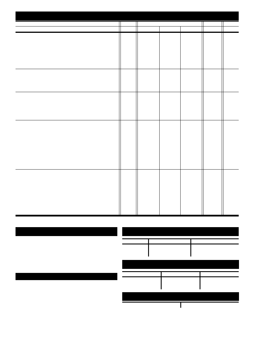
CLC426 Electrical Characteristics
CLC426 Electrical Characteristics
CLC426 Electrical Characteristics (V
(V
(VCC
CC
CC =
=
±±±±±5V; A
5V; A
5V; AVVVVV = +2V/V; R
= +2V/V; R
= +2V/V; Rfffff =100
=100
; R
; RLLLLL = 100
= 100
;;;;; unless noted
unless noted
)))))
A)J-level: spec is 100% tested at +25°C.
1) Minimum stable gain with out external compensation is +2 or
-1V/V, the CLC426 is unity-gain stable with external
compensation.
2) Output is short circuit protected to ground, however maximum
reliability is obtained if output current does not exceed 160mA.
3) See text for compensation techniques.
http://www.national.com
2
supply voltage
±7V
short circuit current
(note 2)
common-mode input voltage
±Vcc
differential input voltage
±10V
maximum junction temperature
+150°C
storage temperature
-65°C to+150°C
lead temperature (soldering 10 sec)
+300°C
ESD rating
2000V
Absolute Maximum Ratings
Notes
PARAMETERS
CONDITIONS
TYP
MIN/MAX RATINGS
UNITS
NOTES
Ambient Temperature
CLC426
+25°C
0 to +70°C -40 to +85°C
FREQUENCY DOMAIN RESPONSE
gain bandwidth product
Vout < 0.5Vpp
230
170
120
100
MHz
-3dB bandwidth, Av=+2
V
out < 0.5Vpp
130
90
70
55
MHz
1
Vout < 5.0Vpp
50
25
22
20
MHz
gain flatness
Vout < 0.5Vpp
peaking
DC to 200MHz
0.6
1.5
2.2
2.5
dB
rolloff
DC to 30MHz
0.0
0.6
1.0
dB
linear phase deviation
DC to 30MHz
0.2
1.0
1.5
°
TIME DOMAIN RESPONSE
rise and fall time
1V step
2.3
3.5
5.0
6.5
ns
settling time
2V step to 0.05%
16
20
24
ns
overshoot
1V step
5
15
18
%
slew rate
5V step
400
300
275
250
V/
s
DISTORTION AND NOISE RESPONSE
2nd harmonic distortion
1V
pp,10MHz
- 62
- 52
- 47
- 45
dBc
3rd harmonic distortion
1Vpp,10MHz
- 68
- 58
- 54
dBc
equivalent input noise
op amp only
voltage
1MHz to 100MHz
1.6
2.0
2.3
2.6
nV/
√Hz
current
1MHz to 100MHz
2.0
3.0
3.6
4.6
pA/
√Hz
STATIC DC PERFORMANCE
open-loop gain
DC
64
60
54
dB
input offset voltage
1.0
2.0
2.8
mV
A
average drift
3
---
10
V/°C
input bias current
5
25
40
65
AA
average drift
90
---
600
700
nA/
°C
input offset current
0.3
3
5
AA
average drift
5
---
25
50
nA/
°C
power-supply rejection ratio
DC
73
65
60
dB
common-mode rejection ratio
DC
70
62
57
dB
supply current
pin #8 open, RL=
∞
11
12
13
15
mA
A
MISCELLANEOUS PERFORMANCE
input resistance
common-mode
500
250
125
k
differential-mode
750
200
50
25
k
input capacitance
common-mode
2.0
3.0
pF
differential-mode
2.0
3.0
pF
output resistance
closed loop
0.07
0.1
0.2
output voltage range
RL=
∞
± 3.8
± 3.5
± 3.3
V
R
L=100
± 3.5
± 3.2
± 2.6
± 1.3
V
input voltage range
common mode
± 3.7
± 3.5
± 3.3
V
output current
± 70
± 50
± 40
+ 35, -20
mA
Min/max ratings are based on product characterization and simulation. Individual parameters are tested as noted. Outgoing quality levels are
determined from tested parameters.
Model
Temperature Range
Description
CLC426AJP
-40°C to +85°C
8-pin PDIP
CLC426AJE
-40°C to +85°C
8-pin SOIC
CLC426A8B
-55°C to +125°C
8-pin CerDIP, MIL-STD-883
Ordering Information
Package
θθθθθ
JC
θθθθθ
JA
Plastic (AJP)
70°C/W
125°C/W
Surface Mount (AJE)
60°C/W
140°C/W
CerDIP
40°C/W
130°C/W
Package Thermal Resistance
Transistor Count
52
Reliability Information
相关PDF资料 |
PDF描述 |
|---|---|
| 5962-9460401MPA | DUAL OP-AMP, 350 uV OFFSET-MAX, 0.08 MHz BAND WIDTH, CDIP8 |
| 5962-9460401MPX | DUAL OP-AMP, 350 uV OFFSET-MAX, 0.08 MHz BAND WIDTH, CDIP8 |
| 5962-9467601MPA | OP-AMP, 10000 uV OFFSET-MAX, CDIP8 |
| 5962-9467601MPA | OP-AMP, 10000 uV OFFSET-MAX, CDIP8 |
| 5962-9469401MPA | OP-AMP, 8000 uV OFFSET-MAX, 80 MHz BAND WIDTH, CDIP8 |
相关代理商/技术参数 |
参数描述 |
|---|---|
| 5962-9459901MXA | 功能描述:NVRAM 8Kbx8 4.5-5.5V 55ns nvSRAM RoHS:否 制造商:Maxim Integrated 数据总线宽度:8 bit 存储容量:1024 Kbit 组织:128 K x 8 接口类型:Parallel 访问时间:70 ns 电源电压-最大:5.5 V 电源电压-最小:4.5 V 工作电流:85 mA 最大工作温度:+ 70 C 最小工作温度:0 C 封装 / 箱体:EDIP 封装:Tube |
| 5962-9459901MXC | 功能描述:NVRAM 8Kbx8 4.5-5.5V 55ns nvSRAM RoHS:否 制造商:Maxim Integrated 数据总线宽度:8 bit 存储容量:1024 Kbit 组织:128 K x 8 接口类型:Parallel 访问时间:70 ns 电源电压-最大:5.5 V 电源电压-最小:4.5 V 工作电流:85 mA 最大工作温度:+ 70 C 最小工作温度:0 C 封装 / 箱体:EDIP 封装:Tube |
| 5962-9459901MXX | 制造商:Cypress Semiconductor 功能描述:NVSRAM28PIN LCC - Bulk |
| 5962-9459901MYA | 功能描述:NVRAM 8Kbx8 4.5-5.5V 55ns nvSRAM RoHS:否 制造商:Maxim Integrated 数据总线宽度:8 bit 存储容量:1024 Kbit 组织:128 K x 8 接口类型:Parallel 访问时间:70 ns 电源电压-最大:5.5 V 电源电压-最小:4.5 V 工作电流:85 mA 最大工作温度:+ 70 C 最小工作温度:0 C 封装 / 箱体:EDIP 封装:Tube |
| 5962-9459902MXA | 制造商:Cypress Semiconductor 功能描述:NVSRAM28PIN SOIC - Bulk |
发布紧急采购,3分钟左右您将得到回复。