- 您现在的位置:买卖IC网 > PDF目录91416 > 5962-9459701MPA (NATIONAL SEMICONDUCTOR CORP) OP-AMP, CDIP8 PDF资料下载
参数资料
| 型号: | 5962-9459701MPA |
| 厂商: | NATIONAL SEMICONDUCTOR CORP |
| 元件分类: | 运算放大器 |
| 英文描述: | OP-AMP, CDIP8 |
| 封装: | DIP-8 |
| 文件页数: | 5/8页 |
| 文件大小: | 1005K |
| 代理商: | 5962-9459701MPA |
Supply Current Adjustment
The CLC426's supply current can be externally adjusted
downward from its nominal value to less than 2mA by
adding an optional resistor (Rp) between pin 8 and the
negative supply as shown in fig 2. The plot labeled "Open-
Loop Gain vs. Supply Current" illustrates the influence
that supply current has over the CLC426's open-loop
response. From the plot it is seen that the CLC426 can be
compensated for unity-gain stability by simply lowering
its supply current. Therefore lowering the CLC426's sup-
ply current effectively reduces its open-loop gain to the
point that there is adequate phase margin at unity gain
crossover. The plot labeled "Supply Current vs. Rp"
provides the means for selecting the value of Rp that
produces the desired supply current. The curve in the plot
represents nominal processing but a ±12% deviation over
process can be expected. The two plots labeled "Voltage
Noise vs. Supply Current" and "Current Noise vs. Supply
Current" illustrate the CLC426 supply current's effect over
its input-referred noise characteristics.
Driving Capacitive Loads
The CLC426 is designed to drive capacitive loads with the
addition of a small series resistor placed between the
output and the load as seen in fig. 3. Two plots located in
the Typical Performance section illustrate this technique
for both frequency domain and time domain applications.
The plot labeled "Frequency Response vs. Capacitive
Load" shows the CLC426's resulting AC response to
various capacitive loads. The values of Rs in this plot
were chosen to maximize the CLC426's AC response
(limited to
≤1dB peaking).
The second plot labeled "Settling Time vs. Capacitive
Load" provides the means for the selection of the value of
Rs which minimizes the CLC426's settling time. As seen
from the plot, for a given capacitive load Rs is chosen from
the curve labeled "Rs". The resulting settling time to
0.05% can then be estimated from the curve labeled "Ts
to 0.05%". The plot of fig. 4 shows the CLC426's pulse
response for various capacitive loads where Rs has been
chosen from the plot labeled "Settling Time vs. Capaci-
tive Load".
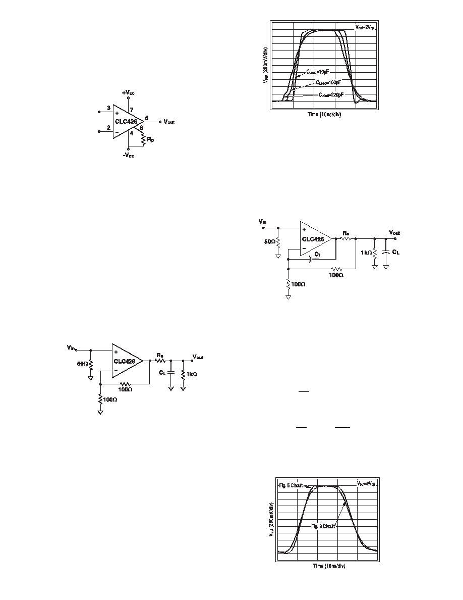
Faster Settling
The circuit of fig. 5 shows an alternative method for driving
capacitive loads that results in quicker settling times. The
small series-resistor, Rs, is used to decouple the CLC426's
open-loop output resistance, Rout, from the load capaci-
tance. The small feedback-capacitance, Cf, is used to
provide a high-frequency bypass between the output and
inverting input. The phase lead introduced by Cf compen-
sates for the phase lag due to CL and therefore restores
stability. The following equations provide values of Rs and
Cf for a given load capacitance and closed-loop amplifier
gain.
Eq. 1
Eq. 2
The plot in
fig. 6 shows
the result of the two methods of capacitive load driving
mentioned above while driving a 100pF||1k
load.
Fig. 2
Fig. 4
Fig. 5
Fig. 3
RR
R
where R
C
R
C
R
s
out
f
g
out
f
g
L
out
g
=
≈
=+
;6
1
2
Fig. 6
5
http://www.national.com
相关PDF资料 |
PDF描述 |
|---|---|
| 5962-9460401MPA | DUAL OP-AMP, 350 uV OFFSET-MAX, 0.08 MHz BAND WIDTH, CDIP8 |
| 5962-9460401MPX | DUAL OP-AMP, 350 uV OFFSET-MAX, 0.08 MHz BAND WIDTH, CDIP8 |
| 5962-9467601MPA | OP-AMP, 10000 uV OFFSET-MAX, CDIP8 |
| 5962-9467601MPA | OP-AMP, 10000 uV OFFSET-MAX, CDIP8 |
| 5962-9469401MPA | OP-AMP, 8000 uV OFFSET-MAX, 80 MHz BAND WIDTH, CDIP8 |
相关代理商/技术参数 |
参数描述 |
|---|---|
| 5962-9459901MXA | 功能描述:NVRAM 8Kbx8 4.5-5.5V 55ns nvSRAM RoHS:否 制造商:Maxim Integrated 数据总线宽度:8 bit 存储容量:1024 Kbit 组织:128 K x 8 接口类型:Parallel 访问时间:70 ns 电源电压-最大:5.5 V 电源电压-最小:4.5 V 工作电流:85 mA 最大工作温度:+ 70 C 最小工作温度:0 C 封装 / 箱体:EDIP 封装:Tube |
| 5962-9459901MXC | 功能描述:NVRAM 8Kbx8 4.5-5.5V 55ns nvSRAM RoHS:否 制造商:Maxim Integrated 数据总线宽度:8 bit 存储容量:1024 Kbit 组织:128 K x 8 接口类型:Parallel 访问时间:70 ns 电源电压-最大:5.5 V 电源电压-最小:4.5 V 工作电流:85 mA 最大工作温度:+ 70 C 最小工作温度:0 C 封装 / 箱体:EDIP 封装:Tube |
| 5962-9459901MXX | 制造商:Cypress Semiconductor 功能描述:NVSRAM28PIN LCC - Bulk |
| 5962-9459901MYA | 功能描述:NVRAM 8Kbx8 4.5-5.5V 55ns nvSRAM RoHS:否 制造商:Maxim Integrated 数据总线宽度:8 bit 存储容量:1024 Kbit 组织:128 K x 8 接口类型:Parallel 访问时间:70 ns 电源电压-最大:5.5 V 电源电压-最小:4.5 V 工作电流:85 mA 最大工作温度:+ 70 C 最小工作温度:0 C 封装 / 箱体:EDIP 封装:Tube |
| 5962-9459902MXA | 制造商:Cypress Semiconductor 功能描述:NVSRAM28PIN SOIC - Bulk |
发布紧急采购,3分钟左右您将得到回复。